
Toshiba Satellite L745 S4210 14 Inch Intel Core I3 Laptop Specifications And Datasheet
Ask AI
— answers from the official manualAnswers from the official manual.
Common questions
Common Questions
10 totalHow do I factory reset the OIS PLUS Series product?
To perform a factory reset, press and hold the Power button for 10 seconds until the LED flashes red. This will clear all settings and return the device to factory defaults; you'll need to re-pair all connected devices after the reset. (Page 23)
What is the correct power supply voltage for an OIS PLUS Series product?
The power supply voltage requirement for an OIS PLUS Series product is +24VDC, with a tolerance of +/-15%. Ensure you provide this exact voltage to avoid damaging the device. (Page 23)
What safety certification does the V200 Series PLC have?
The V200 Series Programmable Controllers are certified with CE and UL marks, meaning they comply with ISO/IEC Guide 22 and EN 45014 standards. (Page 10)
How do I properly mount the OIS PLUS series models?
Panel-mount the OIS PLUS models securely in an upright position in a well-ventilated area without obstructing ventilation openings. Ensure there is adequate clearance as specified by the outline drawings. (Page 5)
What hardware configuration is needed for OIL-DS Configuration Software?
A minimum PC configuration of a Pentium processor with at least 256MB of RAM and Microsoft Windows XP or Vista are required to configure and operate the OIL-DS Configuration software. (Page 13)
What is an example application memory limit for a specific model?
For instance, the OIS20 PLUS model has a maximum Application Memory size of up to 6MB. Always confirm these specifications based on each model you use. (Page 31)
Full Manual
132 pages

UM-OISPLUS-E001
Programmable Logic Controllers
USER’S MANUAL Hardware & Specifications
CONTENTS
###### OIS PLUS Operator Interface Stations
Toshiba International Corporation
Page 1
Thank you for purchasing the OIS PLUS (Operator Interface Stations) product from Toshiba International Corp. OIS PLUS Series products are versatile industrial displays which are configured with Microsoft Windows based software.
Manual’s Purpose and Scope This manual provides information on how to safely install, operate, and maintain your TIC OIS PLUS. This manual includes a section of general safety instructions that describes the warning labels and symbols that are used throughout the manual. Read the manual completely before installing, operating, or performing maintenance on this equipment. This manual and the accompanying drawings should be considered a permanent part of the equipment and should be readily available for reference and review. Dimensions shown in the manual are in metric and/or the English equivalent. Toshiba International Corporation reserves the right, without prior notice, to update information, make product changes, or to discontinue any product or service identified in this publication. TOSHIBA is a registered trademark of the Toshiba Corporation. All other product or trade references appearing in this manual are registered trademarks of their respective owners. Toshiba International Corporation (TIC) shall not be liable for technical or editorial omissions or mistakes in this manual, nor shall it be liable for incidental or consequential damages resulting from the use of information contained in this manual.
This manual is copyrighted. No part of this manual may be photocopied or reproduced in any form without the prior written consent of Toshiba International Corporation.
Toshiba International Corporation. All rights reserved. Printed in the U.S.A.
Page ii
Important Notice The instructions contained in this manual are not intended to cover all details or variations in equipment types, nor may it provide for every possible contingency concerning the installation, operation, or maintenance of this equipment. Should additional information be required contact your Toshiba representative. The contents of this manual shall not become a part of or modify any prior or existing agreement, commitment, or relationship. The sales contract contains the entire obligation of Toshiba International Corporation. The warranty contained in the contract between the parties is the sole warranty of Toshiba International Corporation and any statements contained herein do not create new warranties or modify the existing warranty. Any electrical or mechanical modifications to this equipment without prior written consent of Toshiba International Corporation will void all warranties and may void the 3rd party (CE, UL, CSA, etc) safety certifications. Unauthorized modifications may also result in a safety hazard or equipment damage.
#### Contacting Toshiba’s Customer
Support Center Toshiba’s Customer Support Center may be contacted to obtain help in resolving any system problems that you may experience or to provide application information. The center is open from 8 a.m. to 5 p.m. (CST), Monday through Friday. The Support Center’s toll free number is US 800-231-1412 Fax 713-466-8773 -- Canada 800-5271204 -- Mexico 01-800-527-1204. You may also contact Toshiba by writing to:
Toshiba International Corporation 13131 West Little York Road Houston, Texas 77041-9990 Attn: PLC Marketing
Or email
plc@tic.toshiba.com. For further information on Toshiba’s products and services, please visit our website at www.toshiba.com/ind/.
Page iii
#### Manual Revisions
Please have the following information available when contacting Toshiba International Corp. about this manual.
Name: OIS PLUS User’s Manual: Hardware & Specifications Document: UM-OISPLUS-E001 Revision: Rev No. Date Description
0 2012/02/14 Initial Issue (for OIS PLUS)
#### Related Manuals
Page iv
########## Table of Contents
INTRODUCTION .................................................................................................................................................12 1.1 Purpose of this Manual ............................................................................................................................13

HARDWARE.......................................................................................................................................................19
Page v
BASIC I/O ALLOCATION & SETUP.........................................................................................................................71
HIGH SPEED COUNTER INPUTS ...........................................................................................................................77
PULSE WIDTH MODULATED OUTPUTS ................................................................................................................88
ANALOG MODULE SETUP .................................................................................................................................101
USB HOST OPERATION .....................................................................................................................................104
USB UPLOAD AND DOWNLOAD........................................................................................................................111
USB DRIVER INSTALLATION ..............................................................................................................................117
Page vii
######### 0. General Safety Instructions and Information
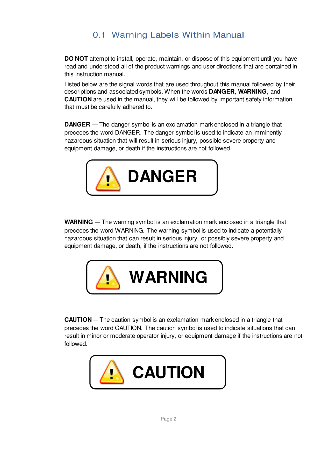
######### 0.1 Warning Labels Within Manual
DO NOT attempt to install, operate, maintain, or dispose of this equipment until you have read and understood all of the product warnings and user directions that are contained in this instruction manual.
Listed below are the signal words that are used throughout this manual followed by their descriptions and associated symbols. When the words DANGER, WARNING, and CAUTION are used in the manual, they will be followed by important safety information that must be carefully adhered to.
DANGER — The danger symbol is an exclamation mark enclosed in a triangle that precedes the word DANGER. The danger symbol is used to indicate an imminently hazardous situation that will result in serious injury, possible severe property and equipment damage, or death if the instructions are not followed.
DANGER


WARNING — The warning symbol is an exclamation mark enclosed in a triangle that precedes the word WARNING. The warning symbol is used to indicate a potentially hazardous situation that can result in serious injury, or possibly severe property and equipment damage, or death, if the instructions are not followed.


WARNING

CAUTION — The caution symbol is an exclamation mark enclosed in a triangle that precedes the word CAUTION. The caution symbol is used to indicate situations that can result in minor or moderate operator injury, or equipment damage if the instructions are not followed.


CAUTION

To identify special hazards, other symbols may appear in conjunction with the DANGER, WARNING, and CAUTION symbols. These warnings describe areas that require special care and/or strict adherence to the procedures to prevent serious injury and possible death.
Electrical Hazard — The electrical hazard symbol is a lightning bolt enclosed in a triangle. The electrical hazard symbol is used to indicate high voltage locations and conditions that may cause serious injury or death if the proper precautions are not observed.
Electrical Hazard


Explosion Hazard — The explosion hazard symbol is an explosion image enclosed in a triangle. The explosion hazard symbol is used to indicate locations and conditions where molten exploding parts may cause serious injury or death if the proper precautions are not observed.
Explosion Hazard


############# 0.2 Equipment Warning Labels.
DO NOT attempt to install, operate, maintain, or dispose of this equipment until you have read and understood all of the product warnings and user directions that are contained in this instruction manual.
Shown below are examples of warning labels that may be found attached to the equipment. DO NOT remove or cover any of the labels. If the labels are damaged or if additional labels are required, contact your Toshiba representative for additional labels. The following are examples of the warning labels that may be found on the equipment and are there to provide useful information or to indicate an imminently hazardous situation that may result in serious injury, severe property and equipment damage, or death if the instructions are not followed.
################ Examples of labels that may be found on the equipment.
############# 0.3 Preparation
Qualified Person
A Qualified Person is one that has the skills and knowledge relating to the construction, installation, operation, and maintenance of the electrical equipment and has received safety training on the hazards involved (Refer to the latest edition of NFPA 70E for additional safety requirements). Qualified Personnel shall:
Equipment Inspection
Disposal
Never dispose of electrical components via incineration. Contact your state environmental agency for details on disposal of electrical components and packaging in your area.
############# 0.4 Installation Precautions
Location and Ambient Requirements
Mounting Requirements
Conductor Routing and Grounding

############ The Metal Of Conduit Is Not An Acceptable Ground.
############# 0.5 Connection, Protection & Setup
Personnel Protection
System Setup Requirements
############# 0.6 System Integration Precautions
The following precautions are provided as general guidelines for using an OIS in an industrial or process control system.
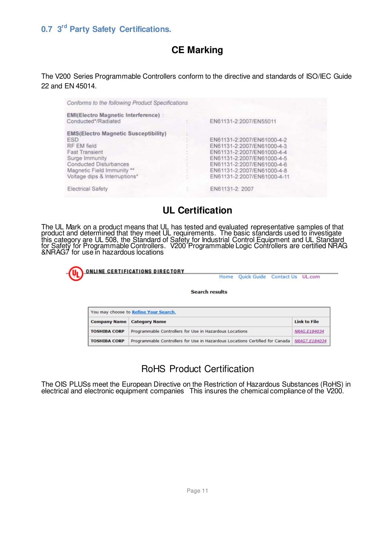
########## 0.7 3rd Party Safety Certifications.CE Marking
The V200 Series Programmable Controllers conform to the directive and standards of ISO/IEC Guide 22 and EN 45014.


########## UL Certification
The UL Mark on a product means that UL has tested and evaluated representative samples of that product and determined that they meet UL requirements. The basic standards used to investigate this category are UL 508, the Standard of Safety for Industrial Control Equipment and UL Standard for Safety for Programmable Controllers. V200 Programmable Logic Controllers are certified NRAG &NRAG7 for use in hazardous locations


########### RoHS Product Certification
The OIS PLUSs meet the European Directive on the Restriction of Hazardous Substances (RoHS) in electrical and electronic equipment companies This insures the chemical compliance of the V200.
######### INTRODUCTION
♦ Purpose of this Manual
OIS PLUS Basics
Hardware Configuration
♦ OIS PLUS Overview
♦ What is an OIS PLUS
♦ How does the OIS PLUS Work?
############# 1.1 Purpose of this Manual
Thank you for purchasing Flexi Panel Series Products. OIS PLUS Series Products are versatile operator interfaces with Microsoft® Windows based configuration Software.
This Manual explains the operation of the OIS PLUS Series and how to implement available features using the OIL-DS Configuration Software. This manual will help you to install, configure and operate your OIS PLUS product.
############## 1.1.1 OIS PLUS Basics
Operator Interface Terminals (OIS PLUSs) provide much more versatility than traditional mechanical control panels. An OIS PLUS allows a plant floor operator to monitor current conditions of a control system and, if necessary, to initiate a change in the operation of the system. OIS PLUSs connect to programmable logic controllers (PLCs) typically through the serial communications port. The OIS PLUS can be programmed to monitor and/or change current values stored in the data memory of the PLC.
OIS PLUSs are having graphics based displays with touch screen and keypad having function keys. Thus OIS PLUS provides much more flexibility in preparing application. Keys can be created in a touch screen OIS PLUS that can be made visible only when needed.
What is a Project? A project is an user created application in OIL-DS Configuration Software. A project contains information such as OIS PLUS model, Network Configuration, Screen information, Task information etc.
What is a Screen? A screen is a visual representation of objects placed on the unit screen. Any partially sized window is usually referred to as a popup screen or window. The user can create his customized screen according to his requirements. Popup windows can also appear on the OIS PLUS display by pressing buttons on the touch screen, The maximum number of screens in an application is only limited by the application memory size. A more in depth discussion on screens is covered in “Screens” section.
What is an Object? An object placed on OIS PLUS screen can perform actions such as displaying text messages, writing a value to a PLC register, or displaying an alarm. An object can be classified as a text or graphical object. A text object is used to display the text on the OIS PLUS and can also be used to perform some action. For example, a data entry object tells the OIS PLUS to continuously monitor a PLC register and allows the user to change the value in the register. Some objects can display graphics whose shape depends on the value of a register. These objects may also change the value of a PLC tag. An example is a Bit Button Object that creates a graphic object on the OIS PLUS. When pressed, it activates a bit in the PLC.
############## 1.1.2 Hardware Requirements
The following basic PC hardware configuration is needed to configure and operate your OIL-DS Configuration Software. Minimal PC configuration for Windows2000 / XP/:
|DEVICE|RECOMMENDED| |---|---| |Processor|800MHz Pentium processor OR equivalent processor| |Operating System|Microsoft Windows 2000 with SP4 Microsoft Windows XP Professional / Home Edition with SP2| |RAM|256MB| |Hard Disk Space Display|800MB (including 200MB for the .NET Framework Redistributable) 1024 x 768 High Color 16-bit| |Mouse/Keyboard|Required|
Minimal PC configuration for Vista/Win7:
|DEVICE|RECOMMENDED| |---|---| |Processor|1GHz Pentium processor or equivalent processor| |Operating System|Microsoft Windows Vista Home and Vista Business edition| |RAM|1GB| |Hard Disk Space|800MB (including 200MB for the .NET Framework Redistributable)| |Display|1024 x 768 High Color 16-bit| |Mouse/Keyboard|Required|
These are the minimum system requirements for a computer running the OIL-DS Configuration software.
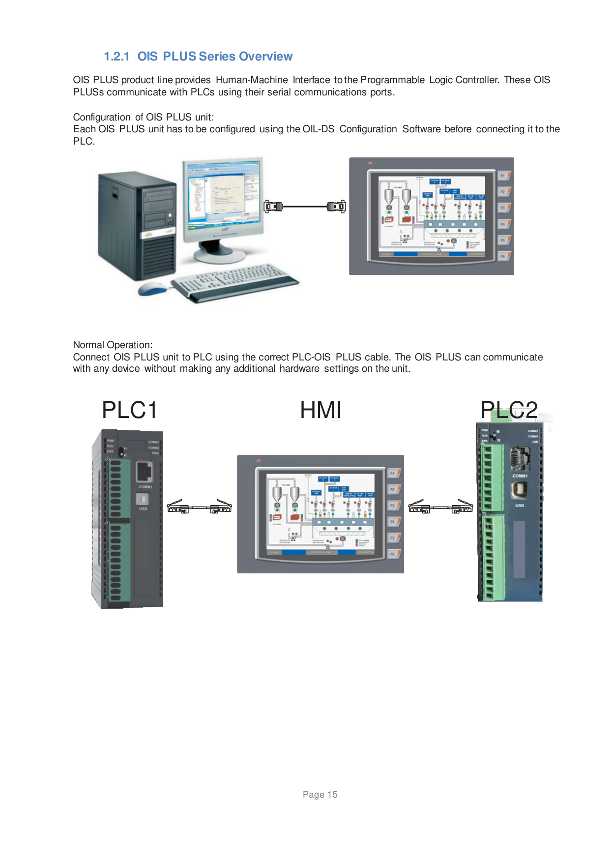
############## 1.2.1 OIS PLUS Series Overview
OIS PLUS product line provides Human-Machine Interface to the Programmable Logic Controller. These OIS PLUSs communicate with PLCs using their serial communications ports.
Configuration of OIS PLUS unit: Each OIS PLUS unit has to be configured using the OIL-DS Configuration Software before connecting it to the PLC.


Normal Operation: Connect OIS PLUS unit to PLC using the correct PLC-OIS PLUS cable. The OIS PLUS can communicate with any device without making any additional hardware settings on the unit.
##### PLC1 HMI PLC2


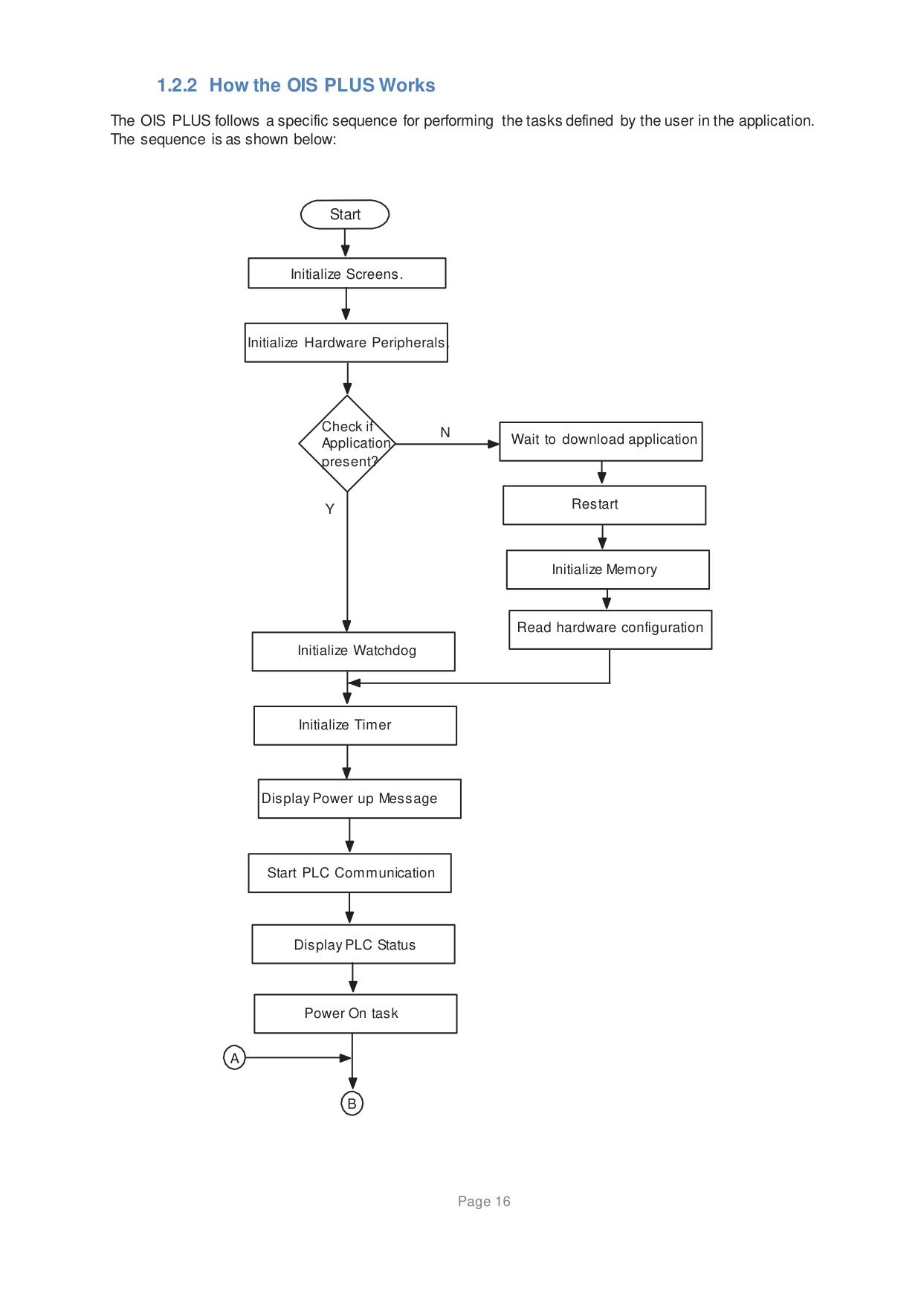
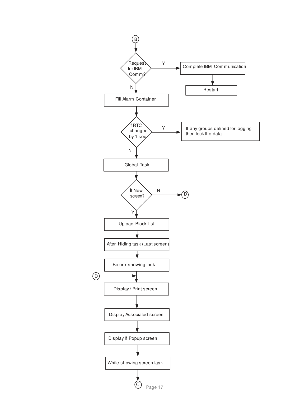
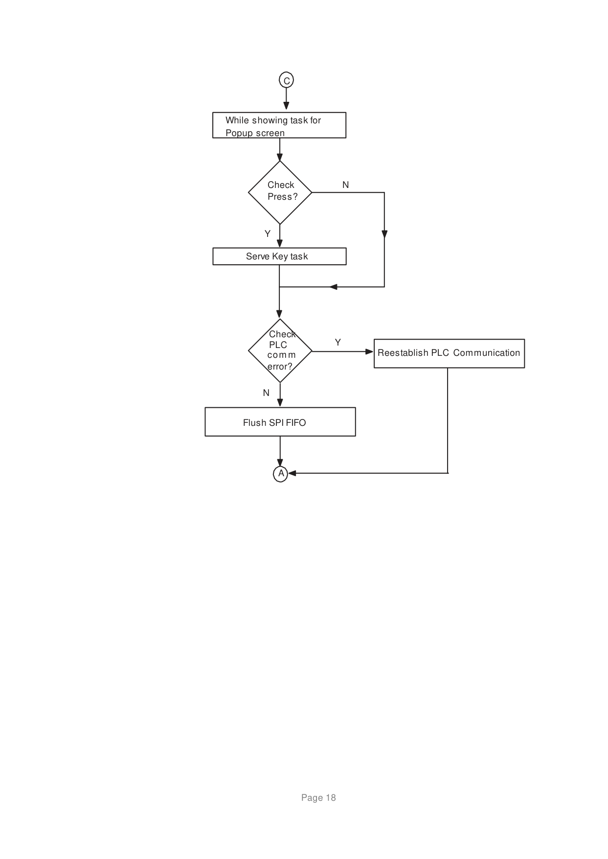
############## 1.2.2 How the OIS PLUS Works
The OIS PLUS follows a specific sequence for performing the tasks defined by the user in the application. The sequence is as shown below:
Start
|Initialize Screens.|Initialize Screens.| |---|---| | | |
|Initialize Hardware Peripherals.| |---|
Check if N Application
present?
Y
|Initialize Watchdog| |---|
A
|Initialize Timer|Initialize Timer| |---|---| | | |
|Display Power up Message|Display Power up Message| |---|---| | | |
|Start PLC Communication|Start PLC Communication| |---|---| | | |
|Display PLC Status|Display PLC Status| |---|---| | | |
|Power On task|Power On task| |---|---| | | |
B
|Wait to download application|Wait to download application| |---|---| | | |

|Restart|Restart| |---|---| | | |
|Initialize Memory|Initialize Memory| |---|---| | | |
Read hardware configuration
B
Request Y for IBM
Comm?
N
|Fill Alarm Container|Fill Alarm Container| |---|---| | | |
If RTC changed
Y by 1 sec
N
|Global Task|Global Task| |---|---| | | |
|Complete IBM Communication|Complete IBM Communication| |---|---| | | |
|Restart| |---|
|If any groups defined for logging then lock the data| |---|
If New N screen? D
Y
|Upload Block list|Upload Block list| |---|---| | | |
|After Hiding task (Last screen)| |---|
D
|Before showing task|Before showing task| |---|---| | | |
|Display / Print screen|Display / Print screen| |---|---| | | |
|Display Associated screen|Display Associated screen| |---|---| | | |
|Display If Popup screen|Display If Popup screen| |---|---| | | |
|While showing screen task|While showing screen task| |---|---| | | |

C
C
|While showing task for Popup screen|While showing task for Popup screen| |---|---| | | |
Check N Press?
Y Serve Key task
Check PLC comm error?
Y
N
|Flush SPI FIFO|Flush SPI FIFO| |---|---| | | |
A
Reestablish PLC Communication
######### HARDWARE
♦ OIS PLUS Models OIS PLUS Models Comparison between OIS PLUS Models
♦ Installation Instructions
Panel cut-out for OIS PLUS Models
Wiring Diagrams
Communication Ports
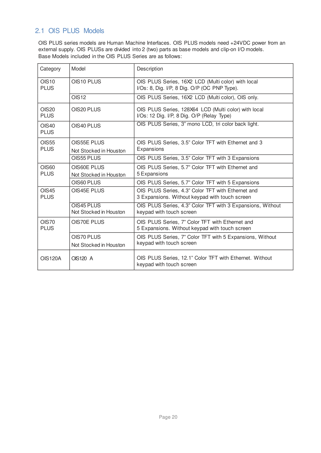
OIS PLUS series models are Human Machine Interfaces. OIS PLUS models need +24VDC power from an external supply. OIS PLUSs are divided into 2 (two) parts as base models and clip-on I/O models. Base Models included in the OIS PLUS Series are as follows:
|Category|Model|Description| |---|---|---| |OIS10 PLUS|OIS10 PLUS|OIS PLUS Series, 16X2 LCD (Multi color) with local I/Os: 8, Dig. I/P, 8 Dig. O/P (OC PNP Type).| |OIS10 PLUS|OIS12|OIS PLUS Series, 16X2 LCD (Multi color), OIS only.| |OIS20 PLUS|OIS20 PLUS|OIS PLUS Series, 128X64 LCD (Multi color) with local I/Os: 12 Dig. I/P, 8 Dig. O/P (Relay Type)| |OIS40 PLUS|OIS40 PLUS|OIS PLUS Series, 3” mono LCD, tri color back light.| |OIS55 PLUS|OIS55E PLUS Not Stocked in Houston|OIS PLUS Series, 3.5” Color TFT with Ethernet and 3 Expansions| |OIS55 PLUS|OIS55 PLUS|OIS PLUS Series, 3.5” Color TFT with 3 Expansions| |OIS60 PLUS|OIS60E PLUS Not Stocked in Houston|OIS PLUS Series, 5.7” Color TFT with Ethernet and 5 Expansions| |OIS60 PLUS|OIS60 PLUS|OIS PLUS Series, 5.7” Color TFT with 5 Expansions|
|OIS45 PLUS
|OIS45E PLUS|OIS PLUS Series, 4.3” Color TFT with Ethernet and 3 Expansions. Without keypad with touch screen| |OIS45 PLUS
|OIS45 PLUS Not Stocked in Houston|OIS PLUS Series, 4.3” Color TFT with 3 Expansions, Without keypad with touch screen| |OIS70 PLUS|OIS70E PLUS|OIS PLUS Series, 7” Color TFT with Ethernet and 5 Expansions. Without keypad with touch screen| |OIS70 PLUS|OIS70 PLUS Not Stocked in Houston|OIS PLUS Series, 7” Color TFT with 5 Expansions, Without keypad with touch screen| |OIS120A|OIS120 A|OIS PLUS Series, 12.1” Color TFT with Ethernet. Without keypad with touch screen|
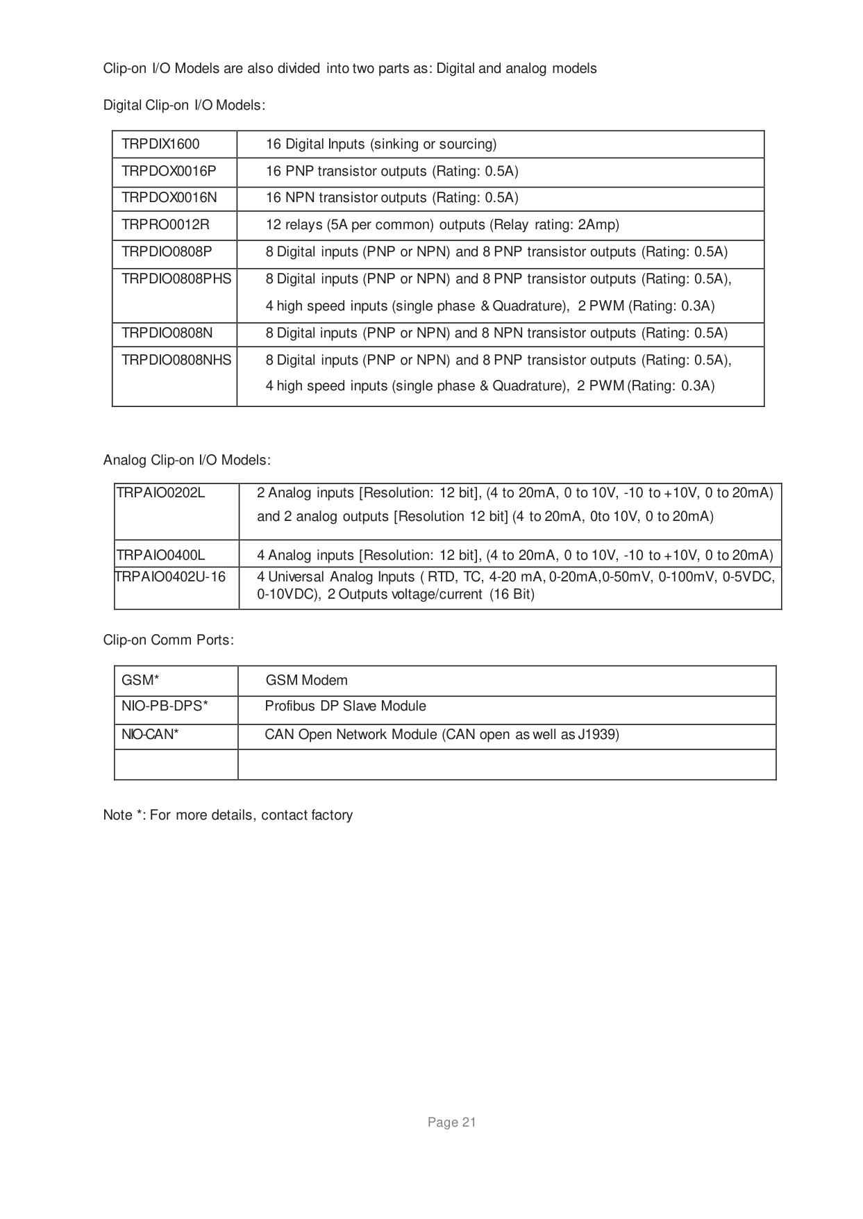
Clip-on I/O Models are also divided into two parts as: Digital and analog models
Digital Clip-on I/O Models:
|TRPDIX1600|16 Digital Inputs (sinking or sourcing)| |---|---| |TRPDOX0016P|16 PNP transistor outputs (Rating: 0.5A)| |TRPDOX0016N|16 NPN transistor outputs (Rating: 0.5A)| |TRPRO0012R|12 relays (5A per common) outputs (Relay rating: 2Amp)| |TRPDIO0808P|8 Digital inputs (PNP or NPN) and 8 PNP transistor outputs (Rating: 0.5A)| |TRPDIO0808PHS|8 Digital inputs (PNP or NPN) and 8 PNP transistor outputs (Rating: 0.5A), 4 high speed inputs (single phase & Quadrature), 2 PWM (Rating: 0.3A)| |TRPDIO0808N|8 Digital inputs (PNP or NPN) and 8 NPN transistor outputs (Rating: 0.5A)| |TRPDIO0808NHS|8 Digital inputs (PNP or NPN) and 8 PNP transistor outputs (Rating: 0.5A), 4 high speed inputs (single phase & Quadrature), 2 PWM (Rating: 0.3A)|
Analog Clip-on I/O Models:
|TRPAIO0202L|2 Analog inputs [Resolution: 12 bit], (4 to 20mA, 0 to 10V, -10 to +10V, 0 to 20mA) and 2 analog outputs [Resolution 12 bit] (4 to 20mA, 0to 10V, 0 to 20mA)| |---|---| |TRPAIO0400L|4 Analog inputs [Resolution: 12 bit], (4 to 20mA, 0 to 10V, -10 to +10V, 0 to 20mA)| |TRPAIO0402U-16|4 Universal Analog Inputs ( RTD, TC, 4-20 mA, 0-20mA,0-50mV, 0-100mV, 0-5VDC, 0-10VDC), 2 Outputs voltage/current (16 Bit)|
Clip-on Comm Ports:
|GSM*|GSM Modem| |---|---| |NIO-PB-DPS*|Profibus DP Slave Module| |NIO-CAN*|CAN Open Network Module (CAN open as well as J1939)| | | |

Note *: For more details, contact factory
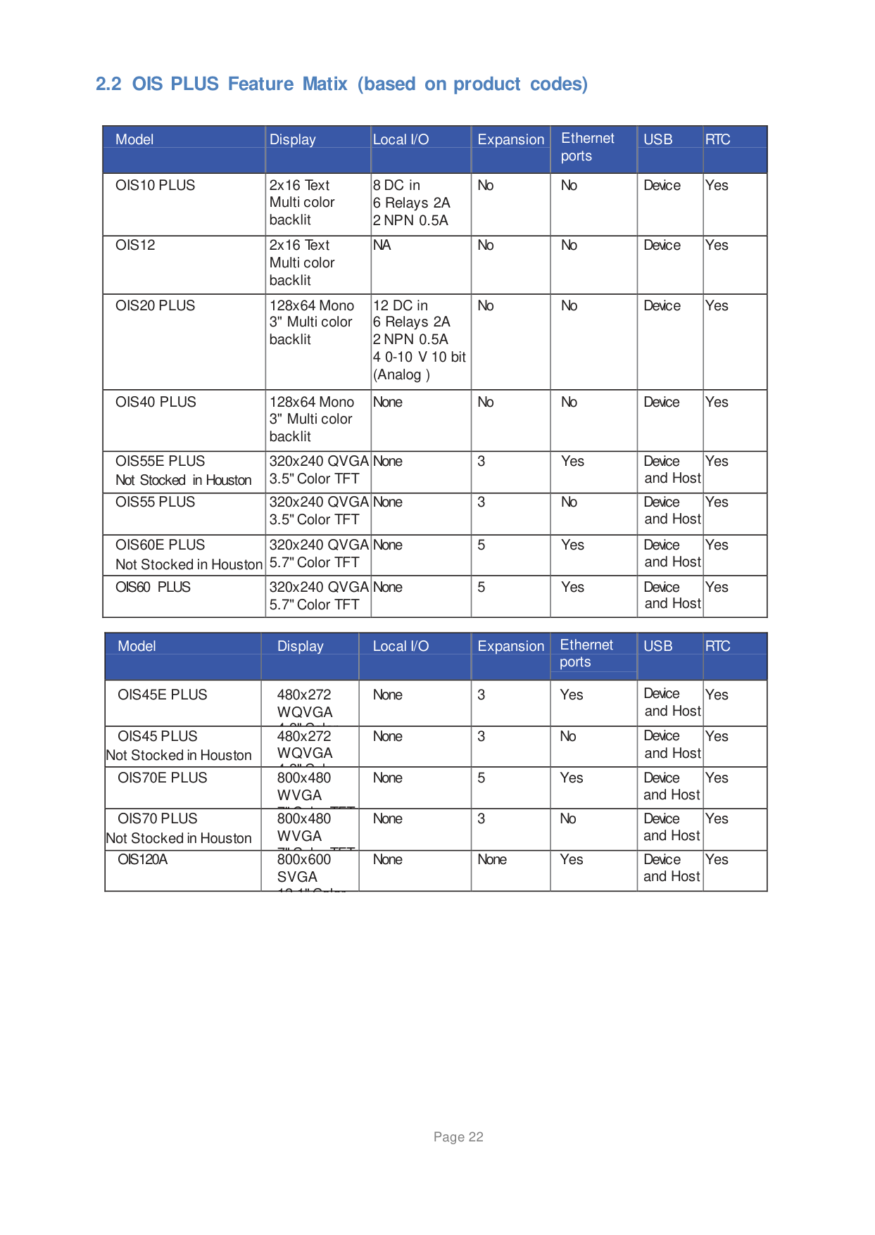
############# 2.2 OIS PLUS Feature Matix (based on product codes)
|Model|Display|Local I/O|Expansion|Ethernet ports
|USB|RTC| |---|---|---|---|---|---|---| |OIS10 PLUS|2x16 Text Multi color backlit|8 DC in 6 Relays 2A 2 NPN 0.5A|No|No|Devic e|Yes| |OIS12|2x16 Text Multi color backlit|NA|No|No|Devic e|Yes| |OIS20 PLUS|128x64 Mono 3" Multi color backlit|12 DC in 6 Relays 2A 2 NPN 0.5A 4 0-10 V 10 bit (Analog )|No|No|Devic e|Yes| |OIS40 PLUS|128x64 Mono 3" Multi color backlit|None|No|No|Device|Yes| |OIS55E PLUS Not Stocked in Houston|320x240 QVGA 3.5" Color TFT|None|3|Yes|Device and Host|Yes| |OIS55 PLUS|320x240 QVGA 3.5" Color TFT|None|3|No|Device and Host|Yes| |OIS60E PLUS Not Stocked in Houston|320x240 QVGA 5.7" Color TFT|None|5|Yes|Device and Host|Yes| |OIS60 PLUS|320x240 QVGA 5.7" Color TFT|None|5|Yes|Device and Host|Yes|
|Model|Display|Local I/O|Expansion|Ethernet ports
|USB|RTC| |---|---|---|---|---|---|---| |OIS45E PLUS|480x272 WQVGA|None|3|Yes|Device and Host|Yes| |OIS45 PLUS Not Stocked in Houston|43" Color 480x272 WQVGA|None|3|No|Device and Host|Yes| |OIS70E PLUS|43" Cl 800x480
WVGA|None|5|Yes|Device and Host|Yes| |OIS70 PLUS Not Stocked in Houston|7" Cl TFT800x480 WVGA|None|3|No|Device and Host|Yes| |OIS120A|7" Cl TFT800x600 SVGA|None|None|Yes|Device and Host|Yes|
12 1" Color
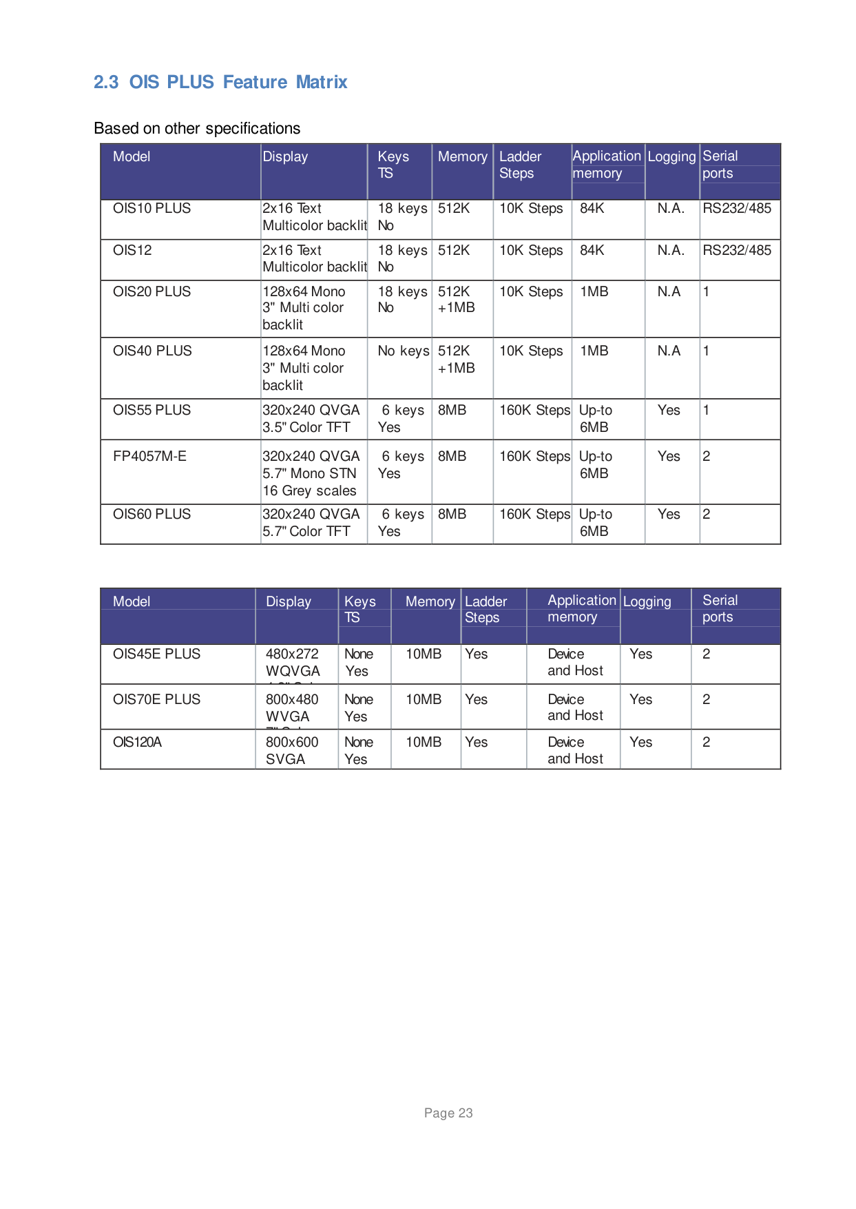
############# 2.3 OIS PLUS Feature Matrix
Based on other specifications
|Model|Display|Keys TS
|Memory|Ladder Steps
|Application memory
|Logging|Serial ports
| |---|---|---|---|---|---|---|---| |OIS10 PLUS|2x16 Text Multicolor backlit|18 keys No|512K|10K Steps|84K|N.A.|RS232/485| |OIS12|2x16 Text Multicolor backlit|18 keys No|512K|10K Steps|84K|N.A.|RS232/485|
|OIS20 PLUS|128x64 Mono 3" Multi color backlit|18 keys No|512K
+1MB|10K Steps|1MB|N.A|1| |OIS40 PLUS|128x64 Mono 3" Multi color backlit|No keys|512K
+1MB|10K Steps|1MB|N.A|1| |OIS55 PLUS|320x240 QVGA 3.5" Color TFT|6 keys Yes|8MB|160K Steps|Up-to 6MB|Yes|1| |FP4057M-E|320x240 QVGA 5.7" Mono STN 16 Grey scales|6 keys Yes|8MB|160K Steps|Up-to 6MB|Yes|2| |OIS60 PLUS|320x240 QVGA 5.7" Color TFT|6 keys Yes|8MB|160K Steps|Up-to 6MB|Yes|2|
|Model|Display|Keys TS
|Memory|Ladder Steps
|Application memory
|Logging|Serial ports
| |---|---|---|---|---|---|---|---| |OIS45E PLUS|480x272 WQVGA|None Yes|10MB|Yes|Device and Host|Yes|2| |OIS70E PLUS|43" Cl 800x480
WVGA|None Yes|10MB|Yes|Device and Host|Yes|2| |OIS120A|7" Cl 800x600
SVGA|None Yes|10MB|Yes|Device and Host|Yes|2|
############# 2.4 OIS PLUS Specifications
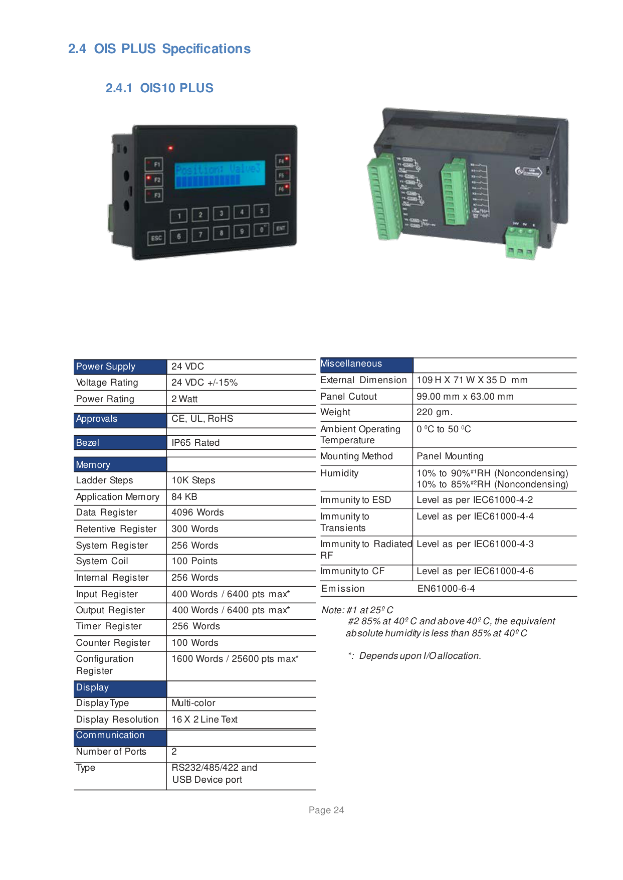
############## 2.4.1 OIS10 PLUS


|Miscellaneous| |---|

|Power Supply|24 VDC| |---|---| |Voltage Rating|24 VDC +/-15%| |Power Rating|2 Watt| | | |
|Approvals|CE, UL, RoHS| | | | |Bezel|IP65 Rated| | | | |Memory| | |Ladder Steps|10K Steps| |Application Memory|84 KB| |Data Register|4096 Words| |Retentive Register|300 Words| |System Register|256 Words| |System Coil|100 Points| |Internal Register|256 Words| |Input Register|400 Words / 6400 pts max*| |Output Register|400 Words / 6400 pts max*| |Timer Register|256 Words| |Counter Register|100 Words| |Configuration Register|1600 Words / 25600 pts max*| |Display| | |Display Type|Multi-color| |Display Resolution|16 X 2 Line Text| |Communication| | |Number of Ports|2| |Type|RS232/485/422 and USB Device port|
External Dimension 109 H X 71 W X 35 D mm Panel Cutout 99.00 mm x 63.00 mm Weight 220 gm. Ambient Operating Temperature
0 0C to 50 C
Mounting Method Panel Mounting Humidity 10% to 90%#1RH (Noncondensing)
10% to 85%#2RH (Noncondensing) Immunity to ESD Level as per IEC61000-4-2 Immunity to Transients
Level as per IEC61000-4-4
Immunity to Radiated RF
Level as per IEC61000-4-3
Immunity to CF Level as per IEC61000-4-6
Emission EN61000-6-4 Note: #1 at 25º C
#2 85% at 40º C and above 40º C, the equivalent absolute humidity is less than 85% at 40º C
*: Depends upon I/O allocation.
Local I/O Specifications for OIS10 PLUS
|Digital Inputs|8 Normal inputs Bidirectional type.| |---|---| | |8 Normal inputs Bidirectional type.| |Digital outputs|6 Relay outputs, 2 PWM / Normal outputs| | | | |Rated Input voltage|NA
| |Rated Input Current|NA| |Input Impedance|NA| |Minimum ON voltage|NA| |Maximum OFF voltage|NA| |Turn ON time|10 msec| |Turn OFF time|10 msec| |Isolation|Optically isolated from the internal circuit| |Connection method|Removable terminals (3.81mm pitch)| | | | |Rated load
|2A at 24VDC| |High Speed Inputs|X1 and X2| |No. of inputs|2 Channels| |Max. Input Frequency|25 KHz| |Max. Input Count|4294967295| | | | |High Speed Outputs|Y6 and Y7| |No. of inputs|2 Channels| |Max. Output Frequency|5 KHz| |Max. Output Count|4294967295|
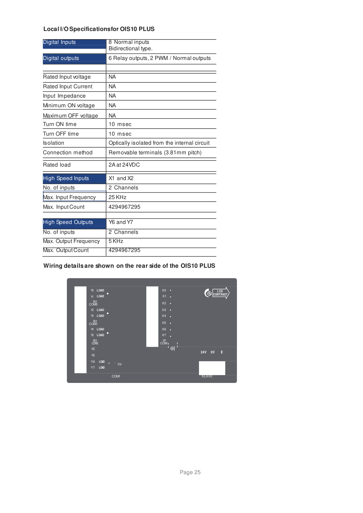
Wiring details are shown on the rear side of the OIS10 PLUS
LOAD LOAD
X0 LCD
CONTRAST X1
LOAD X3 LOAD X4
RLY
X5COM1
LOAD X6 LOAD X7
IP
COM2 NC NC
COM
24V 0V E

+ - 0V
COM1 SLAVE
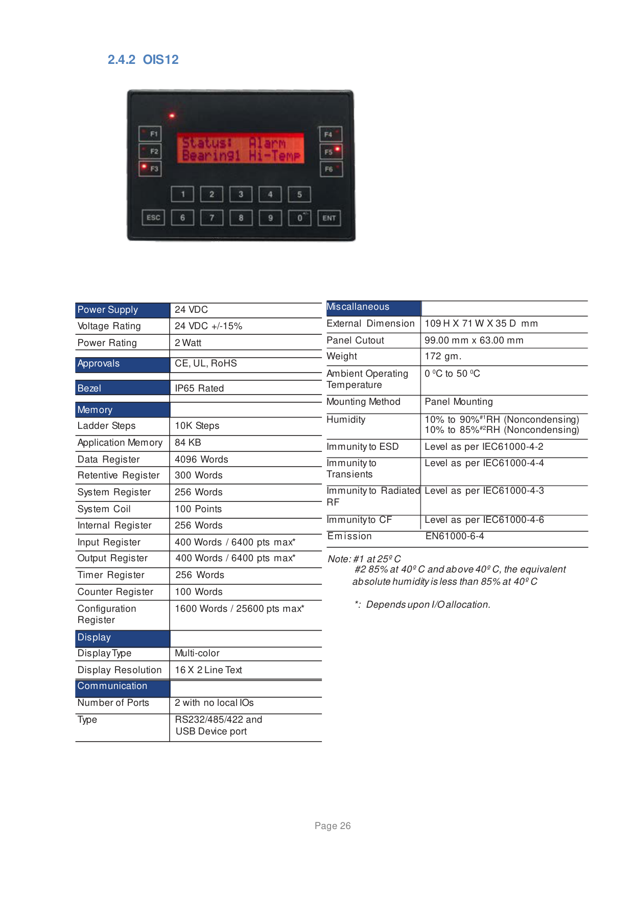
############## 2.4.2 OIS12


|Miscallaneous| |---|

|Power Supply|24 VDC| |---|---| |Voltage Rating|24 VDC +/-15%| |Power Rating|2 Watt| | | | |Approvals|CE, UL, RoHS| | | | |Bezel|IP65 Rated| | | | |Memory| | |Ladder Steps|10K Steps| |Application Memory|84 KB| |Data Register|4096 Words| |Retentive Register|300 Words| |System Register|256 Words| |System Coil|100 Points| |Internal Register|256 Words|
|Input Register|400 Words / 6400 pts max*| |Output Register|400 Words / 6400 pts max*| |Timer Register|256 Words| |Counter Register|100 Words| |Configuration Register|1600 Words / 25600 pts max*| |Display| | |Display Type|Multi-color| |Display Resolution|16 X 2 Line Text| |Communication| | |Number of Ports|2 with no local IOs| |Type|RS232/485/422 and USB Device port|
External Dimension 109 H X 71 W X 35 D mm Panel Cutout 99.00 mm x 63.00 mm Weight 172 gm. Ambient Operating Temperature
0 0C to 50 C
Mounting Method Panel Mounting Humidity 10% to 90%#1RH (Noncondensing)
10% to 85%#2RH (Noncondensing) Immunity to ESD Level as per IEC61000-4-2 Immunity to Transients
Level as per IEC61000-4-4
Immunity to Radiated RF
Level as per IEC61000-4-3
Immunity to CF Level as per IEC61000-4-6 Emission EN61000-6-4
Note: #1 at 25º C
#2 85% at 40º C and above 40º C, the equivalent absolute humidity is less than 85% at 40º C
*: Depends upon I/O allocation.
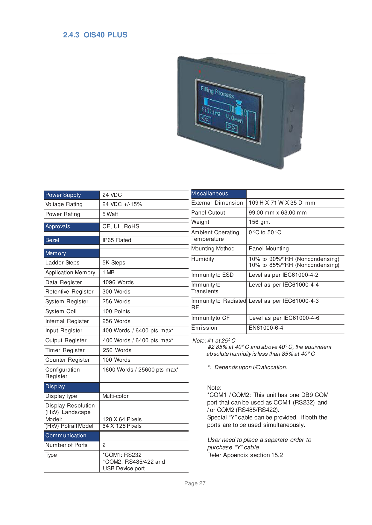
############## 2.4.3 OIS40 PLUS


|Miscallaneous| |---|

|Power Supply|24 VDC| |---|---| |Voltage Rating|24 VDC +/-15%| |Power Rating|5 Watt| | | | |Approvals|CE, UL, RoHS| | | | |Bezel|IP65 Rated| | | | |Memory| | |Ladder Steps|5K Steps| |Application Memory|1 MB| |Data Register|4096 Words| |Retentive Register|300 Words| |System Register|256 Words| |System Coil|100 Points| |Internal Register|256 Words| |Input Register|400 Words / 6400 pts max*| |Output Register|400 Words / 6400 pts max*| |Timer Register|256 Words| |Counter Register|100 Words| |Configuration Register|1600 Words / 25600 pts max*| |Display| | |Display Type|Multi-color| |Display Resolution (HxV) Landscape Model:|128 X 64 Pixels| |(HxV) Potrait Model|64 X 128 Pixels| |Communication| |
|Number of Ports|2| |Type|*COM1: RS232
*COM2: RS485/422 and USB Device port
|
External Dimension 109 H X 71 W X 35 D mm Panel Cutout 99.00 mm x 63.00 mm Weight 156 gm. Ambient Operating Temperature
0 0C to 50 C
Mounting Method Panel Mounting Humidity 10% to 90%#1RH (Noncondensing)
10% to 85%#2RH (Noncondensing) Immunity to ESD Level as per IEC61000-4-2 Immunity to Transients
Level as per IEC61000-4-4
Immunity to Radiated RF
Level as per IEC61000-4-3
Immunity to CF Level as per IEC61000-4-6 Emission EN61000-6-4
Note: #1 at 25º C
#2 85% at 40º C and above 40º C, the equivalent absolute humidity is less than 85% at 40º C
Note:
User need to place a separate order to purchase “Y” cable. Refer Appendix section 15.2
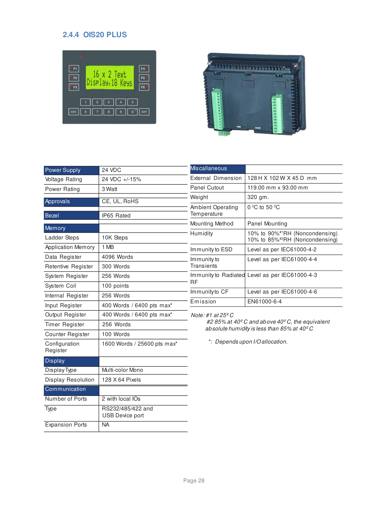
############## 2.4.4 OIS20 PLUS


|Miscallaneous| |---|

|Power Supply|24 VDC| |---|---| |Voltage Rating|24 VDC +/-15%| |Power Rating|3 Watt| | | | |Approvals|CE, UL, RoHS| | | | |Bezel|IP65 Rated| | | | |Memory| | |Ladder Steps|10K Steps| |Application Memory|1 MB| |Data Register|4096 Words| |Retentive Register|300 Words| |System Register|256 Words| |System Coil|100 points| |Internal Register|256 Words| |Input Register|400 Words / 6400 pts max*| |Output Register|400 Words / 6400 pts max*| |Timer Register|256 Words| |Counter Register|100 Words| |Configuration Register|1600 Words / 25600 pts max*| |Display| | |Display Type|Multi-color Mono| |Display Resolution|128 X 64 Pixels|
|Communication| | |Number of Ports|2 with local IOs| |Type|RS232/485/422 and USB Device port| |Expansion Ports|NA|
External Dimension 128 H X 102 W X 45 D mm Panel Cutout 119.00 mm x 93.00 mm Weight 320 gm. Ambient Operating Temperature
0 0C to 50 C
Mounting Method Panel Mounting Humidity 10% to 90%#1RH (Noncondensing)
10% to 85%#2RH (Noncondensing) Immunity to ESD Level as per IEC61000-4-2 Immunity to Transients
Level as per IEC61000-4-4
Immunity to Radiated RF
Level as per IEC61000-4-3
Immunity to CF Level as per IEC61000-4-6 Emission EN61000-6-4
Note: #1 at 25º C
#2 85% at 40º C and above 40º C, the equivalent absolute humidity is less than 85% at 40º C
*: Depends upon I/O allocation.
Local I/O Specifications of OIS20 PLUS
|Digital Inputs|12 Normal inputs Bidirectional type.| |---|---| | |12 Normal inputs Bidirectional type.| |Digital outputs|6 Relay outputs, 2 PWM / Normal outputs| | | | |Rated Input voltage|NA
| |Rated Input Current|NA|
|Input Impedance|NA| |Minimum ON voltage|NA| |Maximum OFF voltage|NA| |Turn ON time|10 msec| |Turn OFF time|10 msec| |Isolation|Optically isolated from the internal circuit| |Connection method|Removable terminals (3.81mm pitch)| | | | |Rated load
|2A at 24VDC| |High Speed Inputs|X1 and X2| |No. of inputs|2 Channels| |Max. Input Frequency|25 KHz| |Max. Input Count|4294967295| | | | |High Speed Outputs|Y6 and Y7| |No. of inputs|2 Channels| |Max. Output Frequency|5 KHz| |Max. Output Count|4294967295|
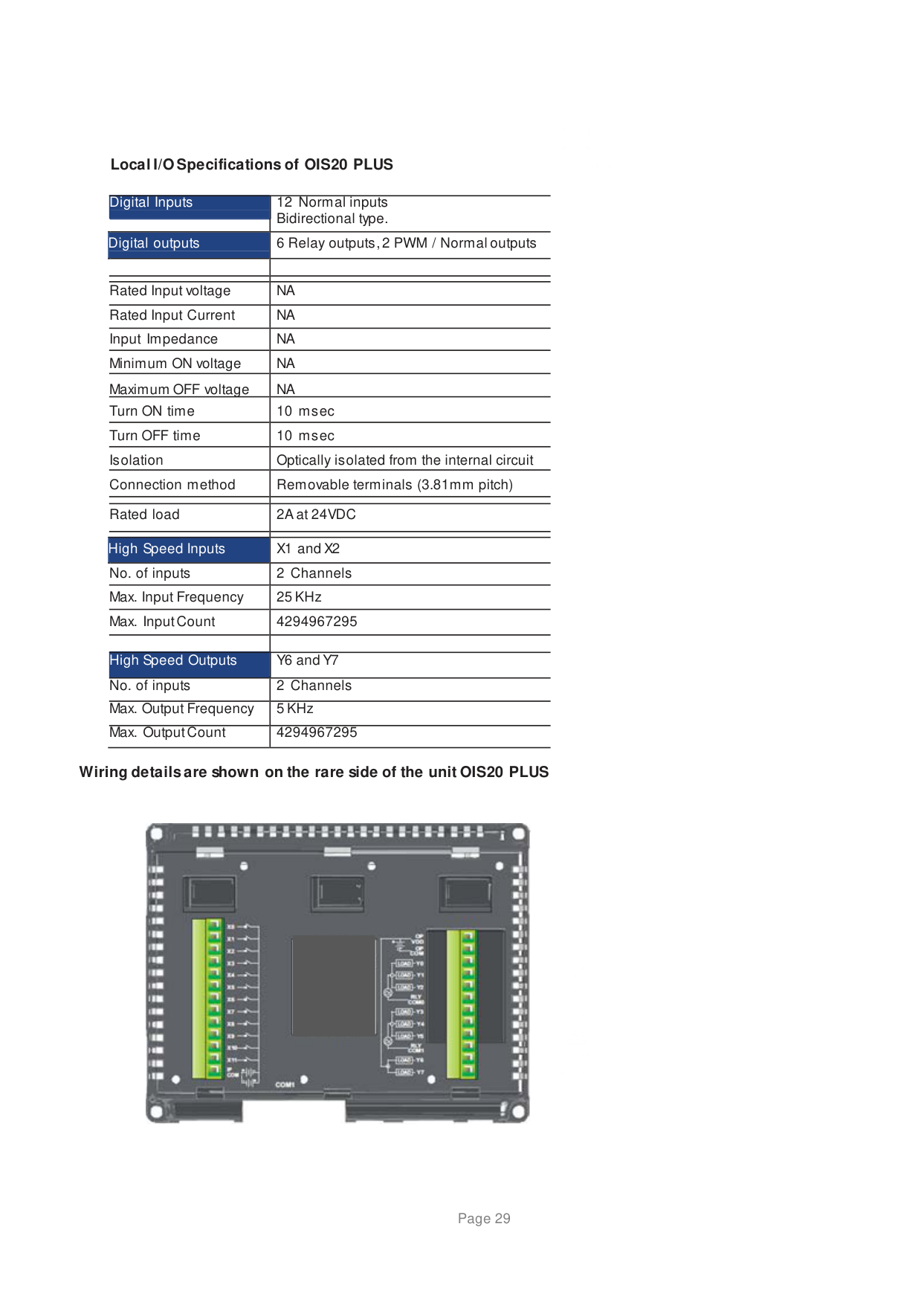
Wiring details are shown on the rare side of the unit OIS20 PLUS


X10
COM
COM1
############## 2.4.5 OIS22 PLUS


Miscallaneous External Dimension 128 H X 102 W X 45 D mm Panel Cutout 119.00 mm x 93.00 mm Weight 265 gm. Ambient Operating Temperature

|Power Supply|24 VDC| |---|---| |Voltage Rating|24 VDC +/-15%| |Power Rating|3 Watt| | | | |Approvals|CE, UL, RoHS| | | | |Bezel|IP65 Rated| | | | |Memory| | |Ladder Steps|10K Steps| |Application Memory|1MB| |Data Register|4096 Words| |Retentive Register|300 Words| |System Register|256 Words| |System Coil|100 points| |Internal Register|256 Words| |Input Register|400 Words / 6400 pts max*| |Output Register|400 Words / 6400 pts max*| |Timer Register|256 Words| |Counter Register|100 Words| |Configuration Register|1600 Words / 25600 pts max*| |Display| | |Display Type|Multi-color| |Display Resolution|128 X 64 Pixels| |Communication| |
|Number of Ports|2| |Type|RS232/485/422 and USB Device port| |Expansion Ports|3|
0 0C to 50 C
Mounting Method Panel Mounting Humidity 10% to 90%#1RH (Noncondensing)
10% to 85%#2RH (Noncondensing) Immunity to ESD Level as per IEC61000-4-2 Immunity to Transients
Level as per IEC61000-4-4
Immunity to Radiated RF
Level as per IEC61000-4-3
Immunity to CF Level as per IEC61000-4-6 Emission EN61000-6-4
Note: #1 at 25º C
#2 85% at 40º C and above 40º C, the equivalent absolute humidity is less than 85% at 40º C
*: Depends upon I/O allocation.
############## 2.4.6 OIS55 PLUS


|Miscallaneous| |---|

|Power Supply|24 VDC| |---|---| |Voltage Rating|24 VDC +/-15%| |Power Rating|4 Watt| | | | |Approvals|CE, UL, RoHS| | | | |Bezel|IP65 Rated| | | | |Memory| | |Total Memory|8MB| |Application Memory|6 MB Max.| |Ladder Steps|160K Steps (1 MB Max.)| |Data Register|4096 Words| |Retentive Register|1400 Words| |System Register|256 Words| |System Coil|100 points| |Internal Register|256 Words| |Input Register|400 Words (max.)| |Output Register|400 Words (max.)| |Timer Register|256 Words| |Counter Register|256 Words| |Configuration Register|1600 Words (max.)| |Time Coils|256 points| |Counter Coils|256 points| |Display| | |Display Size & Type|3.5” TFT Color Display| |Display Resolution|320 X 240 Pixels|
External Dimension 128 H X 102 W X 45 D mm Panel Cutout 119.00 mm x 93.00 mm Weight 285 gm. Ambient Operating Temperature
0 0C to 50 C
Mounting Method Panel Mounting Humidity 10% to 90%#1RH (Noncondensing)
10% to 85%#2RH (Noncondensing) Immunity to ESD Level as per IEC61000-4-2 Immunity to Transients
Level as per IEC61000-4-4
Immunity to Radiated RF
Level as per IEC61000-4-3
Immunity to Surge Level as per IEC61000-4-5 Immunity to CRF Level as per IEC61000-4-6 Emission EN55011 Vibration Tests Frequency 10Hz to 150hz
Displacement +/- 0.35mm Acceleration: 2g Sweep rate : 1 octave per minute Duration : 20 Sweeps / Axis app Axis , X,Y, Z
Shock Test 25 g acceleration with 11 ms 3 Shocks each AXIS (a total of 18 Shocks)
############## 2.4.7 OIS45E PLUS


|Power Supply|24 VDC| |---|---| |Voltage Rating|24 VDC +/-15%| |Power Rating|6 Watt| | | | |Approvals|CE, UL, RoHS| | | | |Bezel|IP66 Rated| | | | |Memory| | |Total Memory|128MB Max. Application| |Memory|Up to 10MB Max.| |Ladder Steps|320K Steps (2MB Max.)| |Data Register|4096 Words| |Retentive Register|1400 Words| |System Register|256 Words| |System Coil|100 points| |Internal Register|256 Words|
|Input Register|400 Words (max.)| |Output Register|400 Words (max.)| |Timer Register|256 Words| |Counter Register|256 Words| |Configuration Register|1600 Words (max.)| |Time Coils|256 points|

Miscallaneous External Dimension 128 H X 102 W X 45 D mm Panel Cutout 119.00 mm x 93.00 mm Weight 330 gm. Ambient Operating Temperature
0 0C to 50 C
Mounting Method Panel Mounting Humidity 10% to 90%#1RH (Noncondensing)
at 40 C Immunity to ESD Level as per IEC61000-4-2 Immunity to Transients
Level as per IEC61000-4-4
Immunity to Radiated RF
Level as per IEC61000-4-3
Immunity to Surge Level as per IEC61000-4-5 Immunity to CRF Level as per IEC61000-4-6 Emission EN55011 Vibration Tests Frequency 10Hz to 150hz
Displacement +/- 0.35mm Acceleration: 2g Sweep rate : 1 octave per minute Duration : 20 Sweeps / Axis app Axis , X,Y, Z
Shock Test 25 g acceleration with 11 ms 3 Shocks each AXIS (a total of 18 Shocks)
|Counter Coils|256 points| |---|---| |Display| | |Display Size & Type|4.3” WQVGA TFT Color Display| |Display Resolution|480 X 272 Pixels| |Touch Screen|Analog Resistive| |Communications| |
|2 COMP Ports|Port 1: RS232 and 1 RS485/422| |2 USB Ports|1 USB Device and 1 USB Host| |Ethernet Port|1 Ethernet Port| |Expansion Port|3| | | | | | |
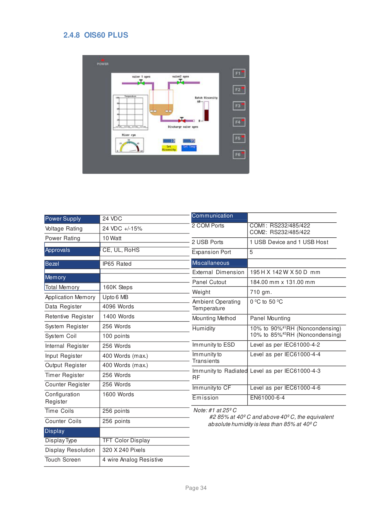
############## 2.4.8 OIS60 PLUS


Communication 2 COM Ports COM1: RS232/485/422
Power Supply 24 VDC Voltage Rating 24 VDC +/-15% Power Rating 10 Watt

COM2: RS232/485/422 2 USB Ports 1 USB Device and 1 USB Host Expansion Port 5 Miscallaneous External Dimension 195 H X 142 W X 50 D mm Panel Cutout 184.00 mm x 131.00 mm Weight 710 gm. Ambient Operating Temperature
|Approvals| |---|
CE, UL, RoHS
| | |---| | | |Memory| |Total Memory|
160K Steps Application Memory Upto 6 MB Data Register 4096 Words Retentive Register 1400 Words System Register 256 Words System Coil 100 points Internal Register 256 Words Input Register 400 Words (max.) Output Register 400 Words (max.) Timer Register 256 Words Counter Register 256 Words Configuration Register
0 0C to 50 0C
Mounting Method Panel Mounting Humidity 10% to 90%#1RH (Noncondensing)
10% to 85%#2RH (Noncondensing) Immunity to ESD Level as per IEC61000-4-2 Immunity to Transients
Level as per IEC61000-4-4
Immunity to Radiated RF
Level as per IEC61000-4-3
Immunity to CF Level as per IEC61000-4-6 Emission EN61000-6-4 Note: #1 at 25º C
1600 Words
Time Coils 256 points Counter Coils 256 points Display
#2 85% at 40º C and above 40º C, the equivalent absolute humidity is less than 85% at 40º C
Display Type TFT Color Display Display Resolution 320 X 240 Pixels Touch Screen 4 wire Analog Resistive
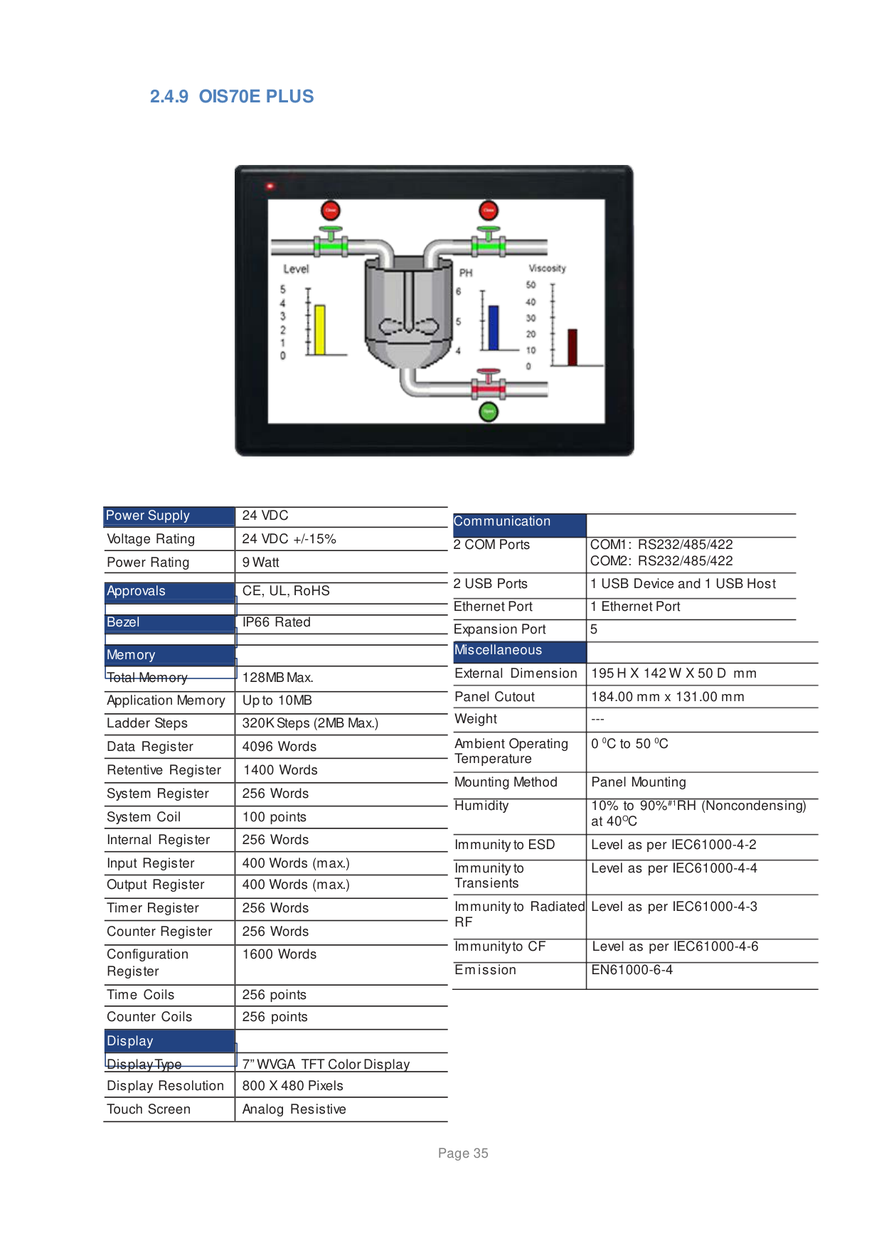
############## 2.4.9 OIS70E PLUS


|Power Supply|24 VDC| |---|---| |Voltage Rating|24 VDC +/-15%| |Power Rating|9 Watt| | | | |Approvals|CE, UL, RoHS|

| | | |Bezel|IP66 Rated| | | | |Memory| | |Total Memory|128MB Max.
| | |128MB Max.
| |Application Memory|Up to 10MB| |Ladder Steps|320K Steps (2MB Max.)| |Data Register|4096 Words| |Retentive Register|1400 Words| |System Register|256 Words| |System Coil|100 points| |Internal Register|256 Words| |Input Register|400 Words (max.)| |Output Register|400 Words (max.)| |Timer Register|256 Words| |Counter Register|256 Words| |Configuration Register|1600 Words| |Time Coils|256 points| |Counter Coils|256 points| |Display| | |Display Type|7” WVGA TFT Color Display
| | |7” WVGA TFT Color Display
| |Display Resolution|800 X 480 Pixels| |Touch Screen|Analog Resistive|
|Communication| |---|

2 COM Ports COM1: RS232/485/422
COM2: RS232/485/422 2 USB Ports 1 USB Device and 1 USB Host Ethernet Port 1 Ethernet Port Expansion Port 5
|Miscellaneous| |---|
External Dimension 195 H X 142 W X 50 D mm Panel Cutout 184.00 mm x 131.00 mm Weight --Ambient Operating Temperature
0 0C to 50 C
Mounting Method Panel Mounting Humidity 10% to 90%#1RH (Noncondensing)
at 40 C Immunity to ESD Level as per IEC61000-4-2 Immunity to Transients
Level as per IEC61000-4-4
Immunity to Radiated RF
Level as per IEC61000-4-3
Immunity to CF Level as per IEC61000-4-6 Emission EN61000-6-4
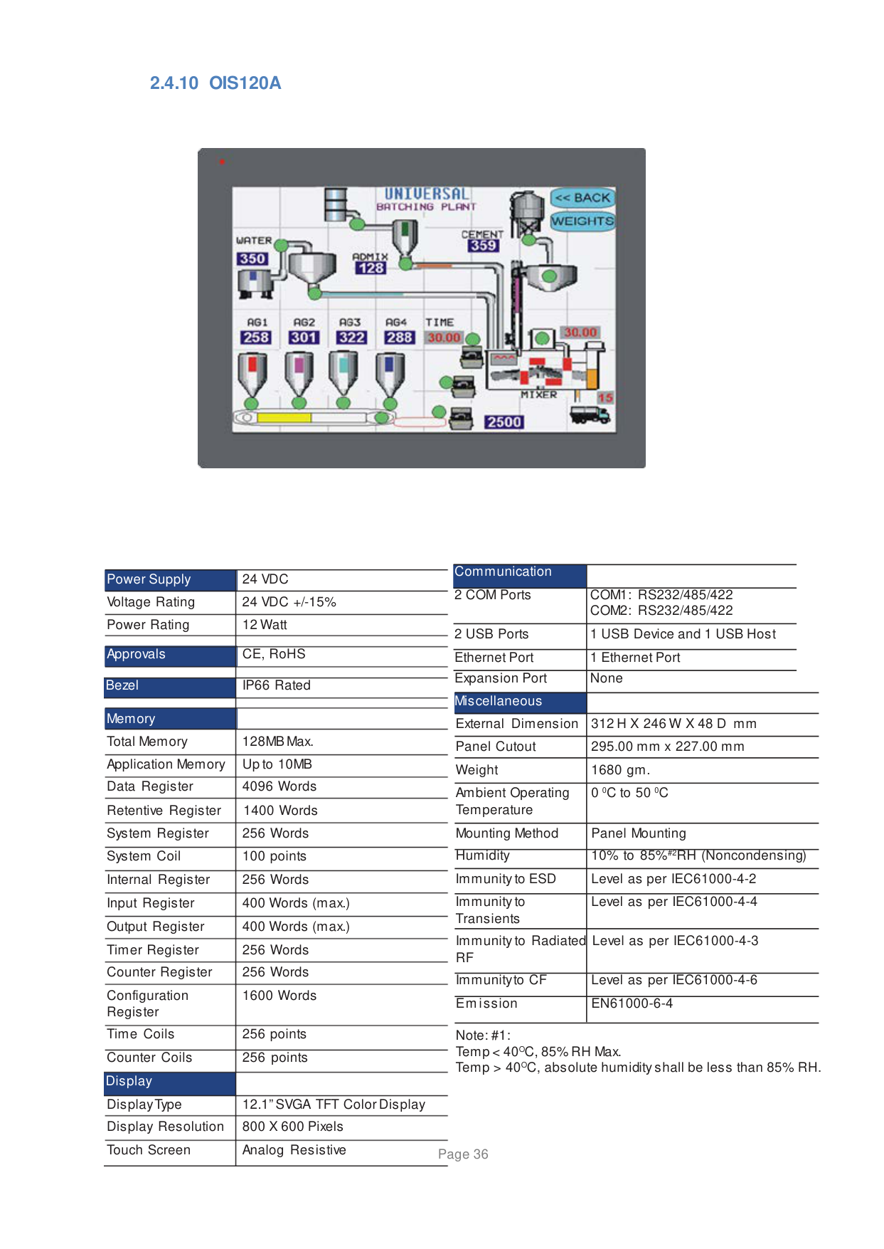
############## 2.4.10 OIS120A


Communication 2 COM Ports COM1: RS232/485/422
|Power Supply| |---|

24 VDC Voltage Rating 24 VDC +/-15% Power Rating 12 Watt
COM2: RS232/485/422 2 USB Ports 1 USB Device and 1 USB Host Ethernet Port 1 Ethernet Port Expansion Port None Miscellaneous External Dimension 312 H X 246 W X 48 D mm Panel Cutout 295.00 mm x 227.00 mm Weight 1680 gm. Ambient Operating 0 0C to 50 0C Temperature Mounting Method Panel Mounting Humidity 10% to 85%#2RH (Noncondensing) Immunity to ESD Level as per IEC61000-4-2 Immunity to Level as per IEC61000-4-4 Transients Immunity to Radiated Level as per IEC61000-4-3 RF Immunity to CF Level as per IEC61000-4-6 Emission EN61000-6-4
CE, RoHS
|Approvals| |---|
|Memory| |---|
Total Memory 128MB Max. Application Memory Up to 10MB Data Register 4096 Words Retentive Register 1400 Words System Register 256 Words System Coil 100 points Internal Register 256 Words Input Register 400 Words (max.) Output Register 400 Words (max.) Timer Register 256 Words Counter Register 256 Words Configuration Register
1600 Words
Time Coils 256 points Counter Coils 256 points Display
Note: #1: Temp < 40OC, 85% RH Max. Temp > 40OC, absolute humidity shall be less than 85% RH.
Display Type 12.1” SVGA TFT Color Display Display Resolution 800 X 600 Pixels Touch Screen Analog Resistive
############# 2.5 OIS PLUS Clip-on I/O Models
Certain displays in the OIS PLUS accept Clip-on I/O modules. Specifications for these modules follow:
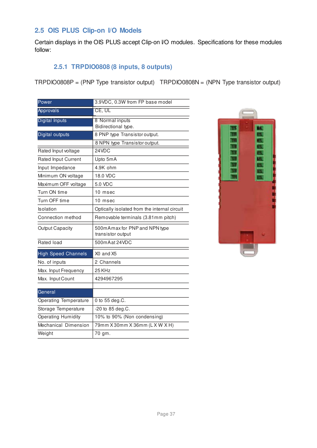
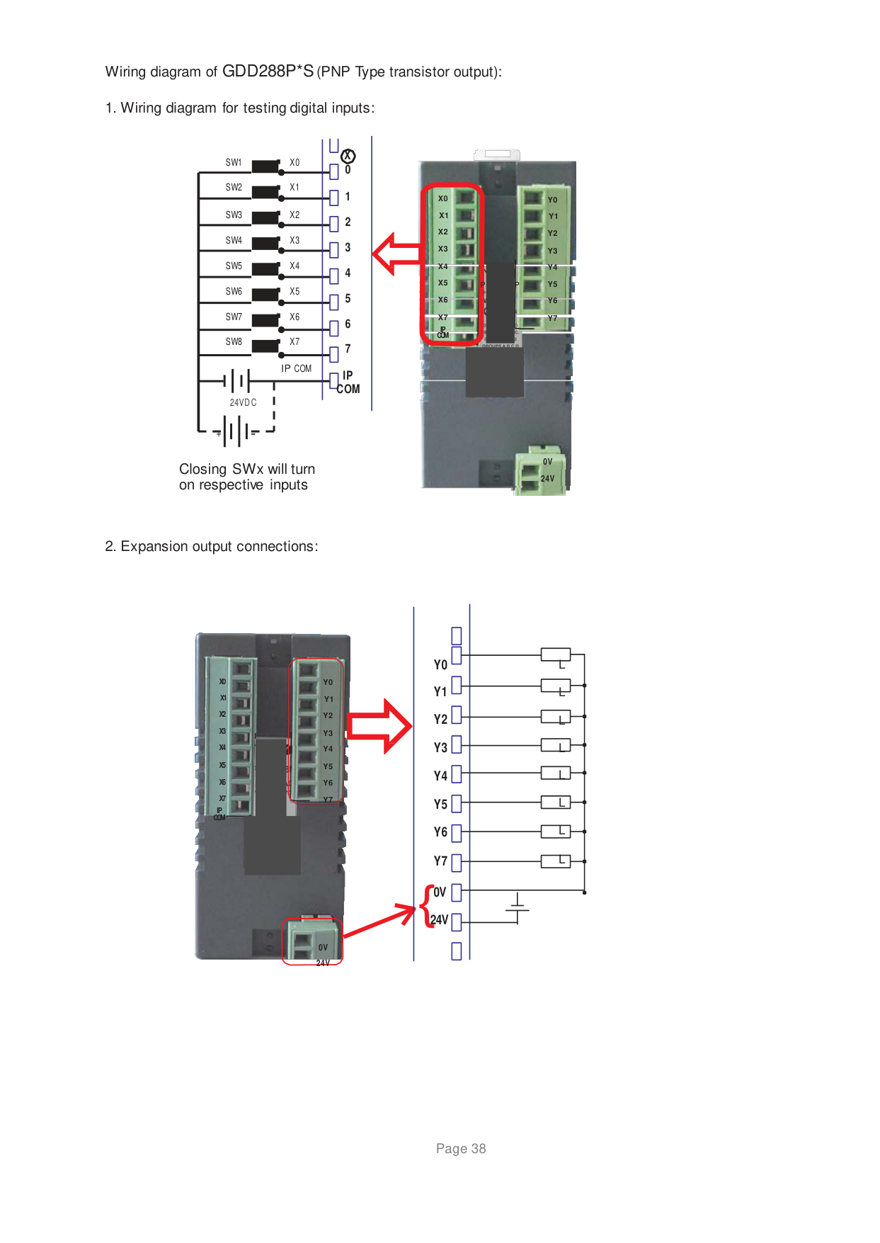
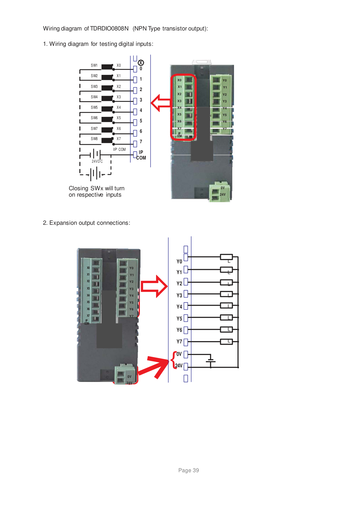
############## 2.5.1 TRPDIO0808 (8 inputs, 8 outputs)
TRPDIO0808P = (PNP Type transistor output) TRPDIO0808N = (NPN Type transistor output)
|Power|3.9VDC, 0.3W from FP base model| |---|---| | | | |Approvals|CE, UL| | | |
|Digital Inputs|8 Normal inputs Bidirectional type.| | |8 Normal inputs Bidirectional type.| |Digital outputs|8 PNP type Transistor output.| | |8 NPN type Transistor output.| | | | |Rated Input voltage|24VDC| |Rated Input Current|Upto 5mA| |Input Impedance|4.9K ohm| |Minimum ON voltage|18.0 VDC| |Maximum OFF voltage|5.0 VDC| |Turn ON time|10 msec| |Turn OFF time|10 msec| |Isolation|Optically isolated from the internal circuit| |Connection method|Removable terminals (3.81mm pitch)| | | | |Output Capacity|500mA max for PNP and NPN type transistor output| |Rated load|500mA at 24VDC| | | | |High Speed Channels|X0 and X5| |No. of inputs|2 Channels| |Max. Input Frequency|25 KHz| |Max. Input Count|4294967295| | | | |General| | |Operating Temperature|0 to 55 deg.C.| |Storage Temperature|-20 to 85 deg.C.| |Operating Humidity|10% to 90% (Non condensing)| |Mechanical Dimension|79mm X 30mm X 36mm (L X W X H)| |Weight|70 gm.|


Wiring diagram of GDD288P*S (PNP Type transistor output):
24VDC
X0 X1 X2 X3 X4 X5 X6 X7 IP COM
X
IP COM
X0 X1 X2 X3 X4 X5 X6 X7 IP COM
PED0808P Y5
H/W
Y6 LISTED Y7
O
. .
0V 24V


X0 X1 X2 X3 X4 X5 X6 X7


IP COM

24V
0V 24V
Wiring diagram of TDRDIO0808N (NPN Type transistor output):
24VDC
X
IP COM
X0 X1 X2 X3 X4 X5 X6 X7 IP COM
PED0808N Y5
H/W
O
. .
0V 24V


|| | |---| | | |---|---| | |L| | |L| | |L| | |L| | |L L| | |L| | |L| | |L| | | | | | | | | |
| | | || | |---| | |


X0 Y0 X1 Y1 X2 Y2 X3 Y3
X0 X1 X2 X3 X4 X5 X6 X7


X4 Y4


X5 Y5


X6 Y6 X7 Y7
IP COM

24V
0V 24V
| | |---|

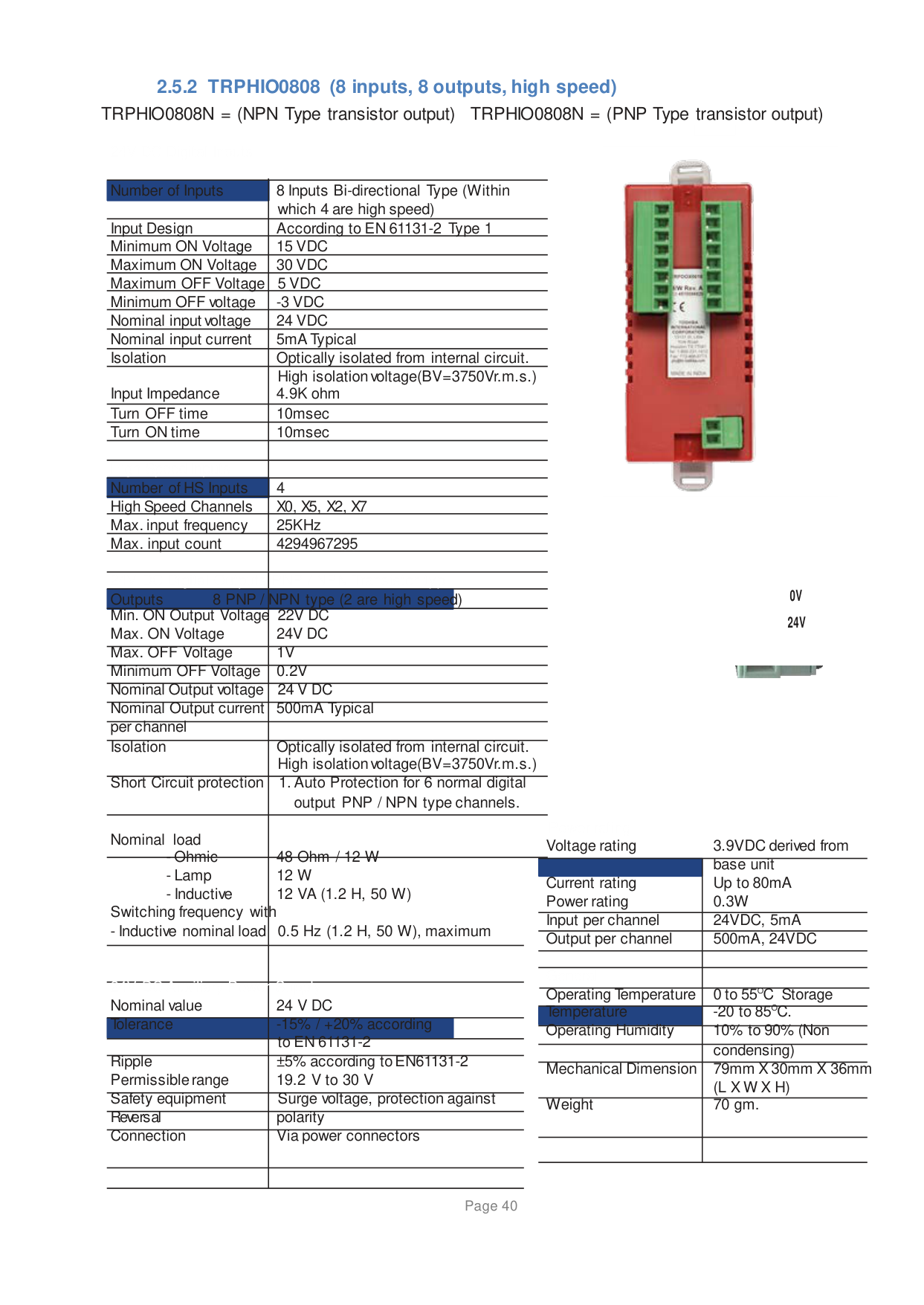
############## 2.5.2 TRPHIO0808 (8 inputs, 8 outputs, high speed)
TRPHIO0808N = (NPN Type transistor output) TRPHIO0808N = (PNP Type transistor output)
Number of Inputs 8 Inputs Bi-directional Type (Within
which 4 are high speed) Input Design According to EN 61131-2 Type 1 Minimum ON Voltage 15 VDC Maximum ON Voltage 30 VDC Maximum OFF Voltage 5 VDC Minimum OFF voltage -3 VDC Nominal input voltage 24 VDC Nominal input current 5mA Typical Isolation Optically isolated from internal circuit.
High isolation voltage(BV=3750Vr.m.s.) Input Impedance 4.9K ohm
Turn OFF time 10msec Turn ON time 10msec
High Speed Inputs Number of HS Inputs 4 High Speed Channels X0, X5, X2, X7 Max. input frequency 25KHz Max. input count 4294967295


X1 X2 X3 X4 X5 X6 X7 IP COM
24V DC Digital Outputs PNP / NPN Transistor typ Outputs 8 PNP / NPN type (2 are high speed) Min. ON Output Voltage 22V DC Max. ON Voltage 24V DC Max. OFF Voltage 1V Minimum OFF Voltage 0.2V Nominal Output voltage 24 V DC Nominal Output current 500mA Typical per channel Isolation Optically isolated from internal circuit.
High isolation voltage(BV=3750Vr.m.s.) Short Circuit protection 1. Auto Protection for 6 normal digital
output PNP / NPN type channels.
################## 0V 24V

Nominal load
Switching frequency with
24V DC Auxiliary Power Supply Nominal value 24 V DC Tolerance -15% / +20% according
to EN 61131-2 Ripple ±5% according to EN61131-2 Permissible range 19.2 V to 30 V Safety equipment Surge voltage, protection against Reve rs al polarity Connection Via power connectors
Voltage rating 3.9VDC derived from
base unit Current rating Up to 80mA Power rating 0.3W Input per channel 24VDC, 5mA Output per channel 500mA, 24VDC
General Operating Temperature 0 to 55OC Storage Temperature -20 to 85OC. Operating Humidity 10% to 90% (Non
condensing) Mechanical Dimension 79mm X 30mm X 36mm
(L X W X H) Weight 70 gm.
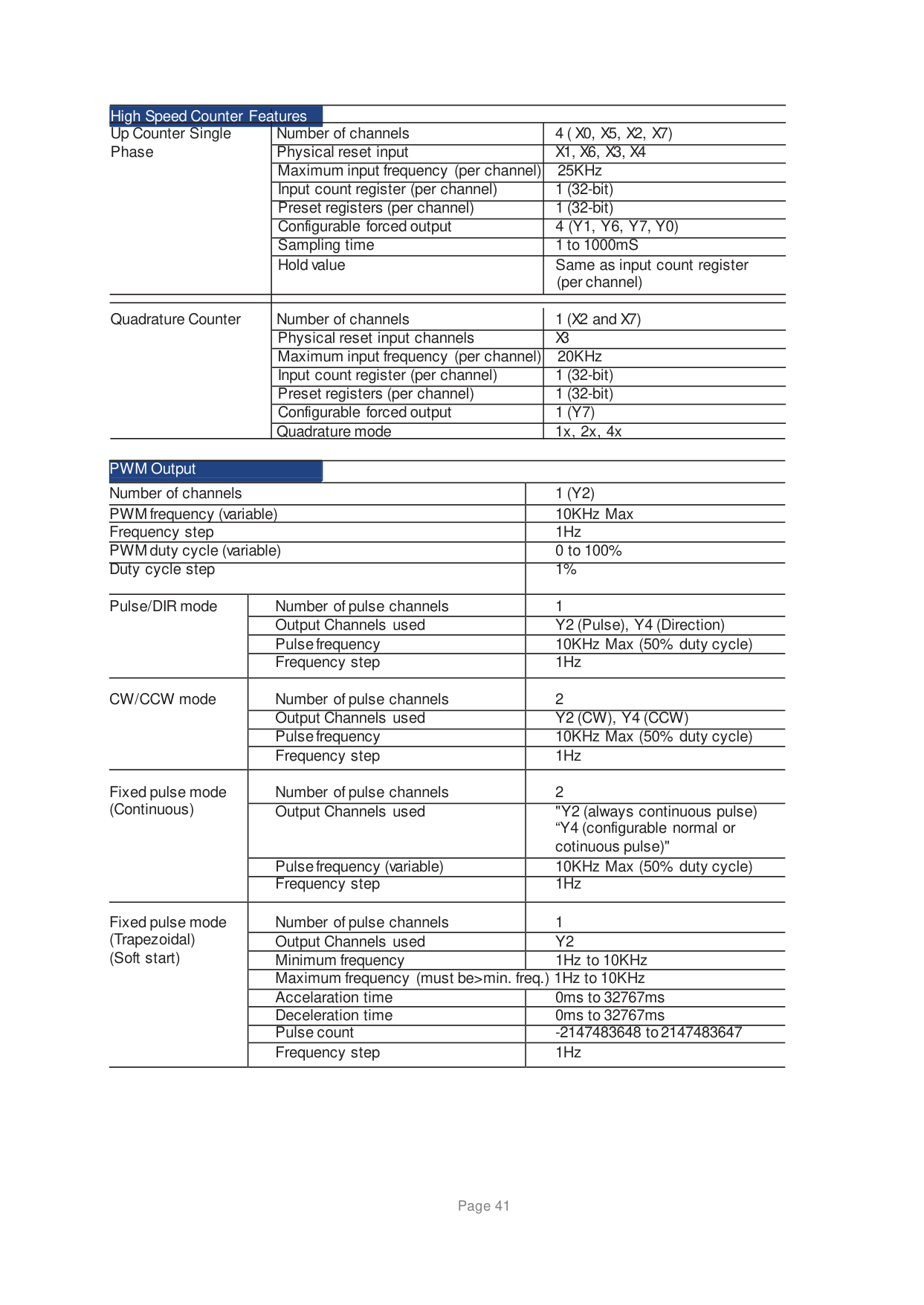
High Speed Counter Features Up Counter Single Number of channels 4 ( X0, X5, X2, X7) Phase Physical reset input X1, X6, X3, X4
Maximum input frequency (per channel) 25KHz Input count register (per channel) 1 (32-bit) Preset registers (per channel) 1 (32-bit) Configurable forced output 4 (Y1, Y6, Y7, Y0) Sampling time 1 to 1000mS Hold value Same as input count register
(per channel)
Quadrature Counter Number of channels 1 (X2 and X7) Physical reset input channels X3 Maximum input frequency (per channel) 20KHz Input count register (per channel) 1 (32-bit) Preset registers (per channel) 1 (32-bit) Configurable forced output 1 (Y7) Quadrature mode 1x, 2x, 4x
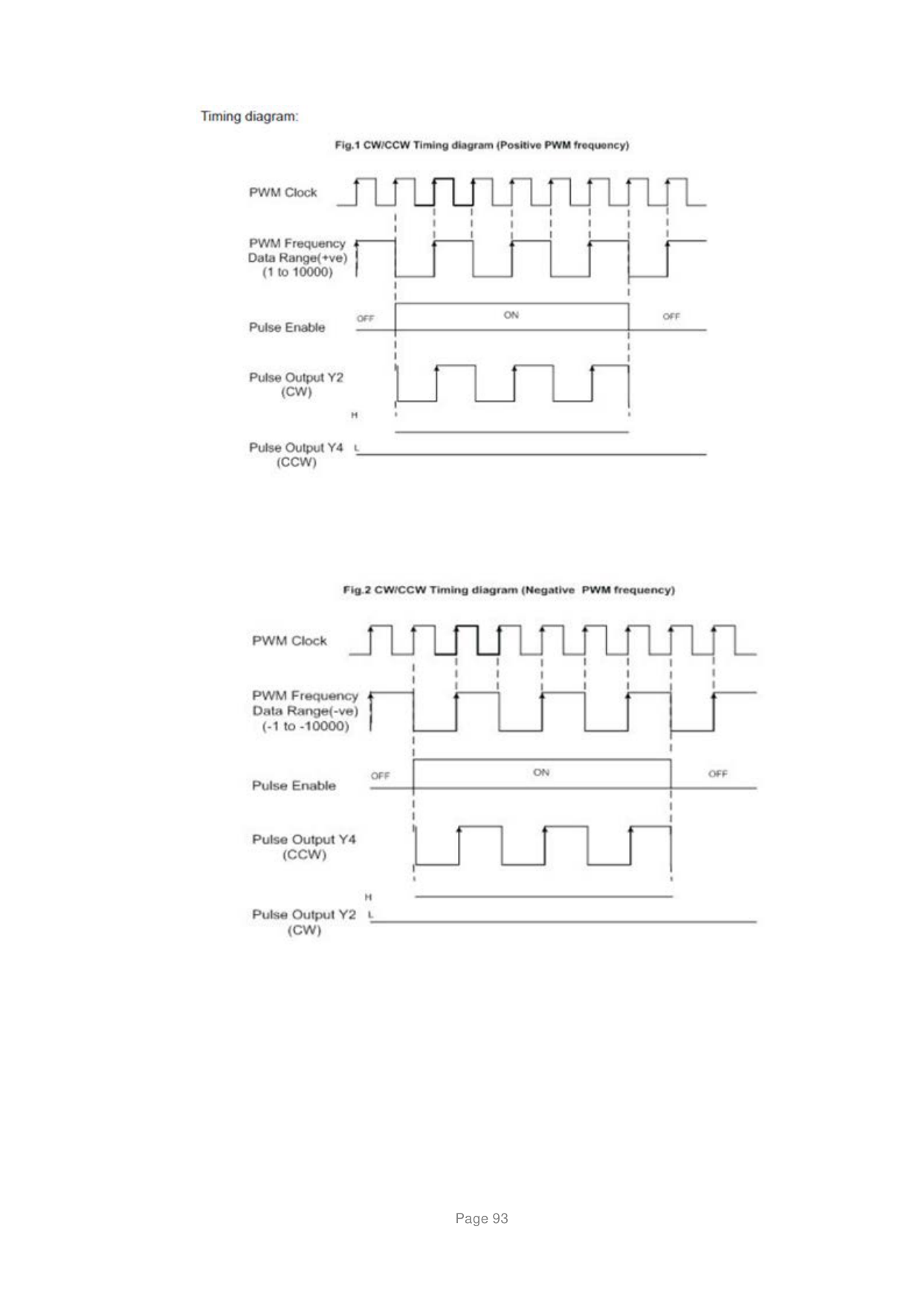
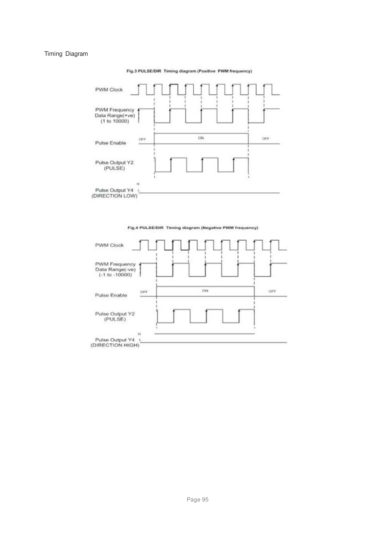
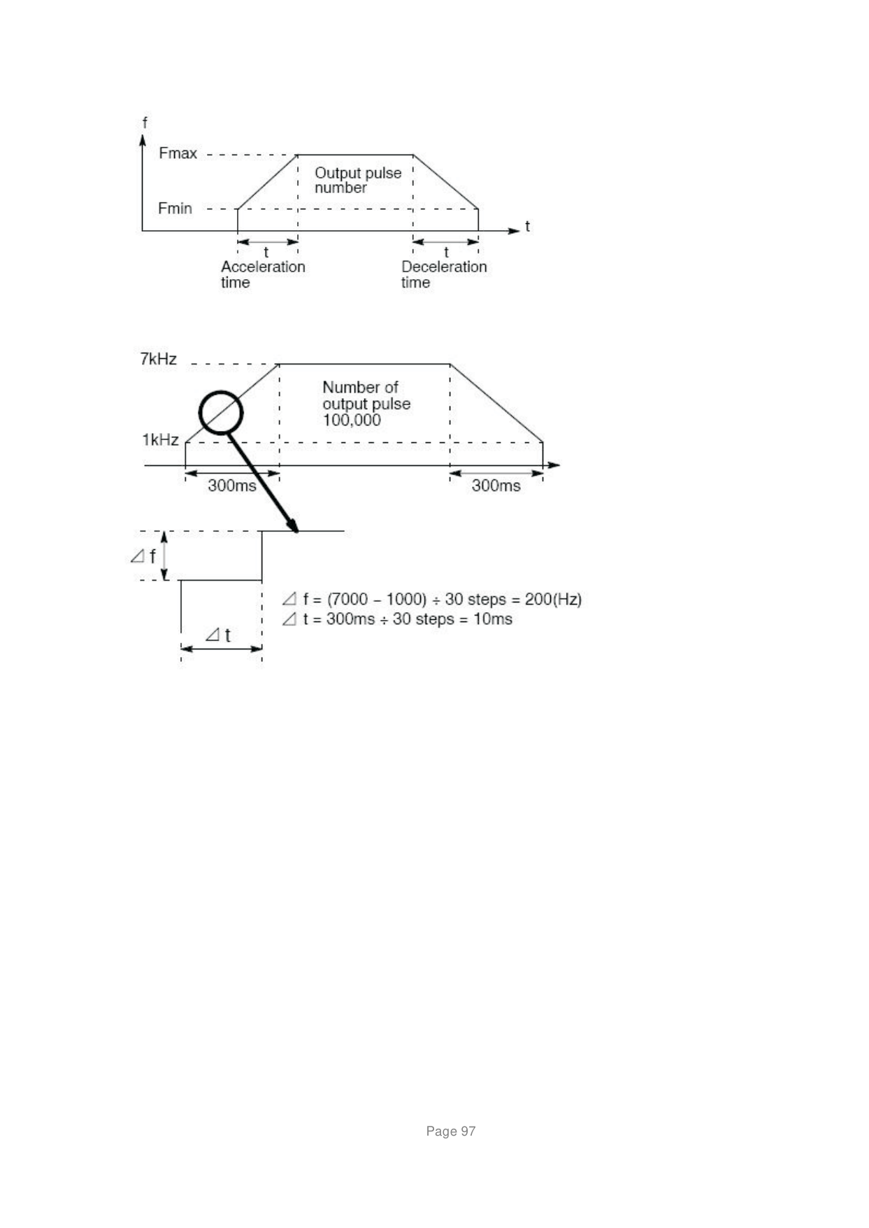
|PWM Output|PWM Output| | | |---|---|---|---| |Number of channels|Number of channels|Number of channels|1 (Y2)| |PWM frequency (variable)|PWM frequency (variable)|PWM frequency (variable)|10KHz Max| |Frequency step|Frequency step|Frequency step|1Hz| |PWM duty cycle (variable)|PWM duty cycle (variable)|PWM duty cycle (variable)|0 to 100%| |Duty cycle step|Duty cycle step|Duty cycle step|1%| |Pulse/DIR mode
|Number of pulse channels|Number of pulse channels|1| |Pulse/DIR mode
|Output Channels used|Output Channels used|Y2 (Pulse), Y4 (Direction)| |Pulse/DIR mode
|Pulse frequency|Pulse frequency|10KHz Max (50% duty cycle)| |Pulse/DIR mode
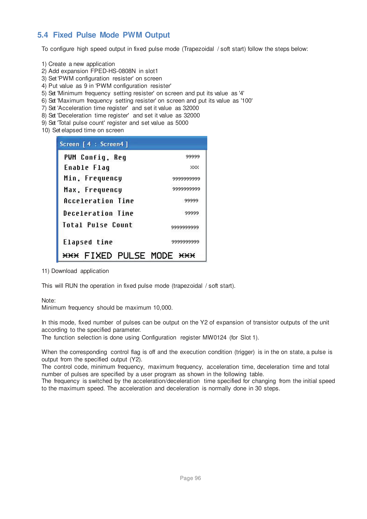
|Frequency step|Frequency step|1Hz| |CW/CCW mode|Number of pulse channels Output Channels used|Number of pulse channels Output Channels used|2 Y2 (CW), Y4 (CCW)| |CW/CCW mode| | | | |CW/CCW mode|Pulse frequency|Pulse frequency|10KHz Max (50% duty cycle)| |CW/CCW mode|Frequency step|Frequency step|1Hz| |Fixed pulse mode (Continuous)|Number of pulse channels|Number of pulse channels|2| |Fixed pulse mode (Continuous)|Output Channels used|Output Channels used|"Y2 (always continuous pulse) “Y4 (configurable normal or cotinuous pulse)"|
|Fixed pulse mode (Continuous)|Pulse frequency (variable)|Pulse frequency (variable)|10KHz Max (50% duty cycle)| |Fixed pulse mode (Continuous)|Frequency step|Frequency step|1Hz| |Fixed pulse mode (Trapezoidal) (Soft start)
|Number of pulse channels|Number of pulse channels|1| |Fixed pulse mode (Trapezoidal) (Soft start)
|Output Channels used|Output Channels used|Y2| |Fixed pulse mode (Trapezoidal) (Soft start)
|Minimum frequency|Minimum frequency|1Hz to 10KHz| |Fixed pulse mode (Trapezoidal) (Soft start)
|Maximum frequency (must be>min. freq.) 1Hz to 10KHz|Maximum frequency (must be>min. freq.) 1Hz to 10KHz|Maximum frequency (must be>min. freq.) 1Hz to 10KHz| |Fixed pulse mode (Trapezoidal) (Soft start)
|Accelaration time|Accelaration time|0ms to 32767ms| |Fixed pulse mode (Trapezoidal) (Soft start)
|Deceleration time|Deceleration time|0ms to 32767ms| |Fixed pulse mode (Trapezoidal) (Soft start)
|Pulse count|Pulse count|-2147483648 to 2147483647| |Fixed pulse mode (Trapezoidal) (Soft start)
|Frequency step|Frequency step|1Hz|
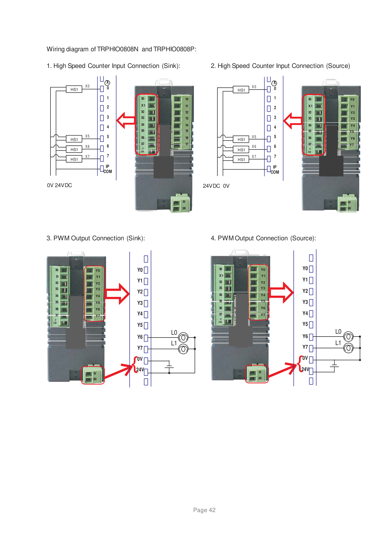
Wiring diagram of TRPHIO0808N and TRPHIO0808P:
X


X
X0 HS1
X0 HS1
X0 X1 X2 X3 X4 X5 X6 X7
X0 X1 X2 X3 X4 X5 X6 X7


PED0808N Y5 H/W Rev. A5
PED0808N Y5 H/W Rev. A5
Y6 LISTED Y7
49RN
I P COM
I P COM


IP COM
IP COM
0V 24VDC
24VDC 0V
0V 24V
0V 24V

X0 X1 X2 X3 X4 X5 X6 X7 I P COM


Rev. A5
LISTED


X0 X1 X2 X3 X4 X5 X6 X7


PED0808P Rev. A5
##################### LISTED 49RN
I P COM
O

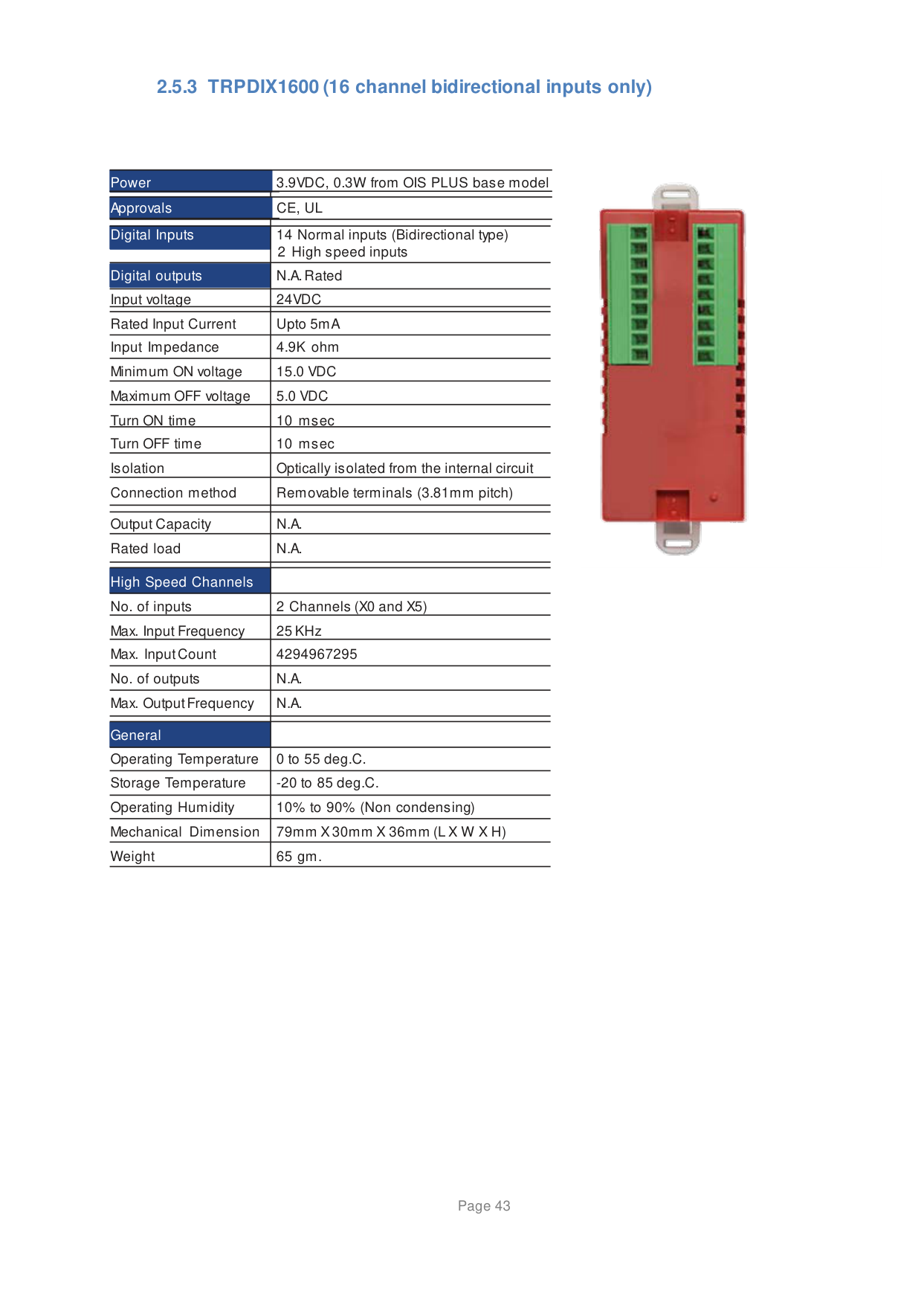
############## 2.5.3 TRPDIX1600 (16 channel bidirectional inputs only)
|Power|3.9VDC, 0.3W from OIS PLUS base model| |---|---| | | | |Approvals|CE, UL| | | | |Digital Inputs|14 Normal inputs (Bidirectional type) 2 High speed inputs| | |14 Normal inputs (Bidirectional type) 2 High speed inputs| |Digital outputs|N.A. Rated| |Input voltage|24VDC|
| | | |Rated Input Current|Upto 5mA| |Input Impedance|4.9K ohm| |Minimum ON voltage|15.0 VDC| |Maximum OFF voltage|5.0 VDC| |Turn ON time|10 msec| |Turn OFF time|10 msec| |Isolation|Optically isolated from the internal circuit| |Connection method|Removable terminals (3.81mm pitch)| | | | |Output Capacity|N.A.| |Rated load|N.A.| | | | |High Speed Channels| | |No. of inputs|2 Channels (X0 and X5)| |Max. Input Frequency|25 KHz| |Max. Input Count|4294967295| |No. of outputs|N.A.| |Max. Output Frequency|N.A.| | | | |General| | |Operating Temperature|0 to 55 deg.C.| |Storage Temperature|-20 to 85 deg.C.| |Operating Humidity|10% to 90% (Non condensing)| |Mechanical Dimension|79mm X 30mm X 36mm (L X W X H)| |Weight|65 gm.|


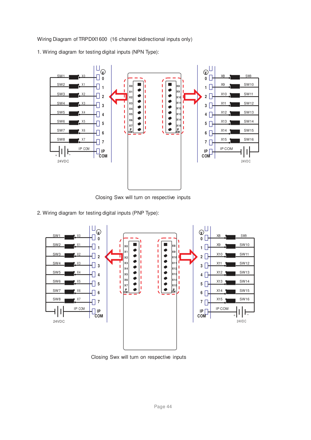
Wiring Diagram of TRPDIX1600 (16 channel bidirectional inputs only)
+ 24VDC
X0 X1 X2 X3 X4 X5 X6 X7 IP COM
X
IP COM
X0 X1 X2 X3 X4 X5 X6 X7 IP
COM
X8 X9
IP COM
X
IP COM
X8 X9
IP COM
24VDC
Closing Swx will turn on respective inputs
24VDC
X
IP COM
X0 X1 X2 X3 X4 X5 X6 X7 IP
COM
X8 X9
IP COM
X
IP COM
IP COM
+ 24VDC
Closing Swx will turn on respective inputs
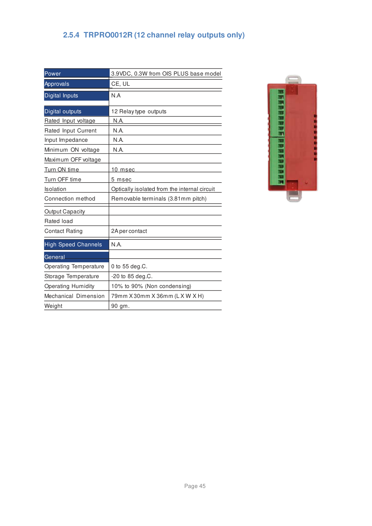
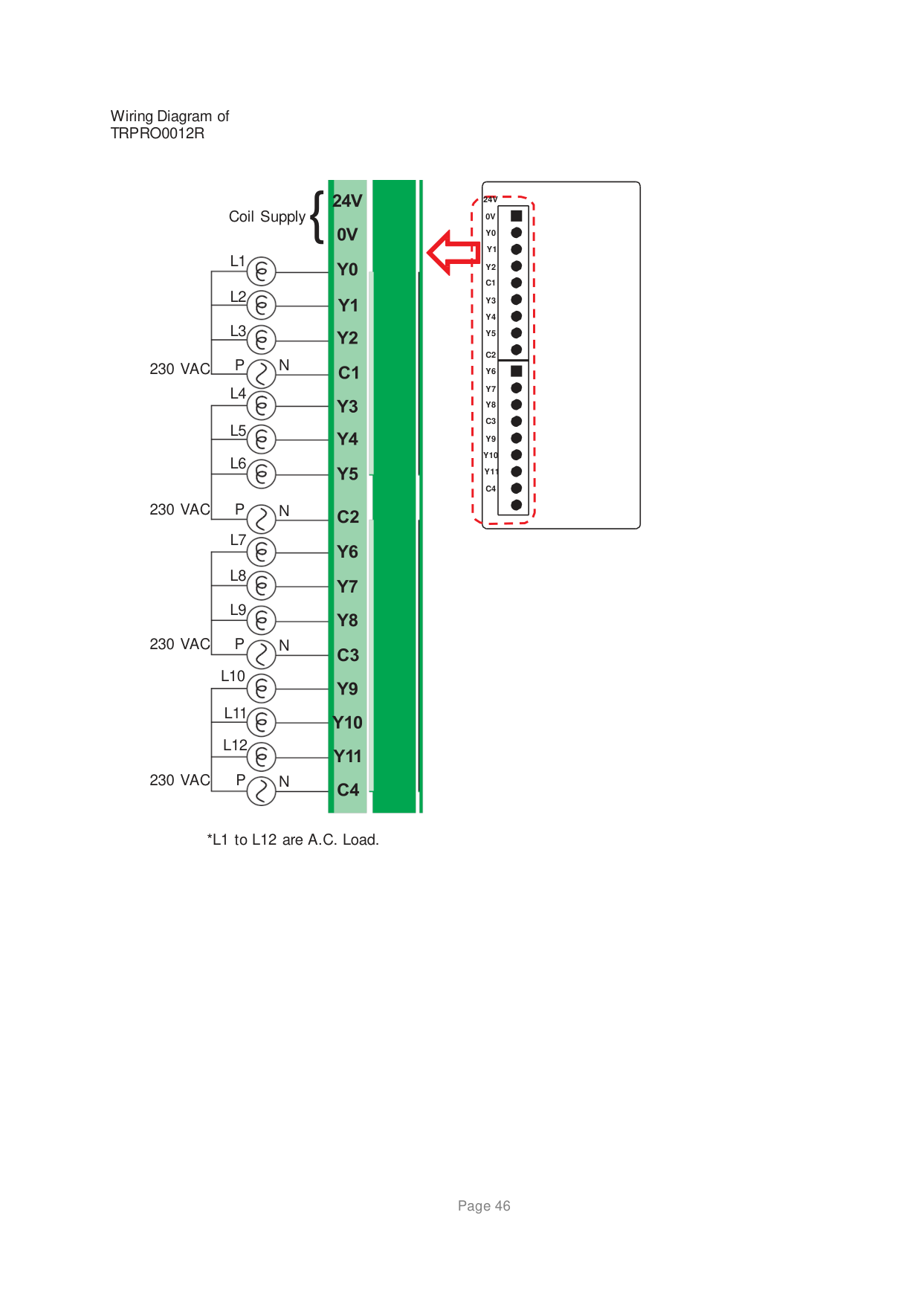
############## 2.5.4 TRPRO0012R (12 channel relay outputs only)
|Power|3.9VDC, 0.3W from OIS PLUS base model| |---|---| | | | |Approvals|CE, UL| | | | |Digital Inputs|N.A|
| |N.A| |Digital outputs|12 Relay type outputs| |Rated Input voltage|N.A.| | | | |Rated Input Current|N.A.| |Input Impedance|N.A.| |Minimum ON voltage|N.A.| |Maximum OFF voltage| | |Turn ON time|10 msec| |Turn OFF time|5 msec| |Isolation|Optically isolated from the internal circuit| |Connection method|Removable terminals (3.81mm pitch)| | | | |Output Capacity| | |Rated load| | |Contact Rating|2A per contact| | | | |High Speed Channels|N.A.| | | | |General| | | |0 to 55 deg.C.| |Operating Temperature|0 to 55 deg.C.| |Storage Temperature|-20 to 85 deg.C.| |Operating Humidity|10% to 90% (Non condensing)| |Mechanical Dimension|79mm X 30mm X 36mm (L X W X H)| |Weight|90 gm.|


Wiring Diagram of TRPRO0012R
Coil Supply{ L1 L2 L3

24V 0V
| | |---| | |
C2

N
230 VAC P L4
L5 L6
230 VAC P L7
N
L8 L9
230 VAC P
N
230 VAC
N
*L1 to L12 are A.C. Load.
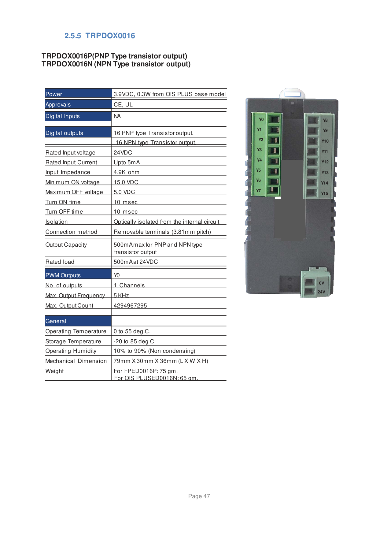
############## 2.5.5 TRPDOX0016
################ TRPDOX0016P(PNP Type transistor output) TRPDOX0016N (NPN Type transistor output)
|Power|3.9VDC, 0.3W from OIS PLUS base model| |---|---| | | | |Approvals|CE, UL| | | | |Digital Inputs|NA| | |NA| |Digital outputs|16 PNP type Transistor output.| | |16 NPN type Transistor output.| | | | |Rated Input voltage|24VDC| |Rated Input Current|Upto 5mA| |Input Impedance|4.9K ohm| |Minimum ON voltage|15.0 VDC| |Maximum OFF voltage|5.0 VDC|
|Turn ON time|10 msec| |Turn OFF time|10 msec| |Isolation|Optically isolated from the internal circuit| |Connection method|Removable terminals (3.81mm pitch)| | | | |Output Capacity|500mA max for PNP and NPN type transistor output| |Rated load|500mA at 24VDC| | | | |PWM Outputs|Y0| |No. of outputs|1 Channels| |Max. Output Frequency|5 KHz| |Max. Output Count|4294967295| | | | |General| | |Operating Temperature|0 to 55 deg.C.| |Storage Temperature|-20 to 85 deg.C.| |Operating Humidity|10% to 90% (Non condensing)| |Mechanical Dimension|79mm X 30mm X 36mm (L X W X H)| |Weight|For FPED0016P: 75 gm. For OIS PLUSED0016N: 65 gm.|


0V 24V

Wiring Diagram of TRPDOX0016P:

LOAD
LOAD Y3
LOAD Y5

LOAD
LOAD
LOAD


LOAD

LOAD

LOAD


LOAD
+ 24V +


Wiring Diagram of TRPDOX0016N:

LOAD
LOAD

LOAD
LOAD
LOAD
LOAD
LOAD
LOAD


LOAD
LOAD

LOAD
LOAD LOAD LOAD

LOAD


LOAD
+ +


24V

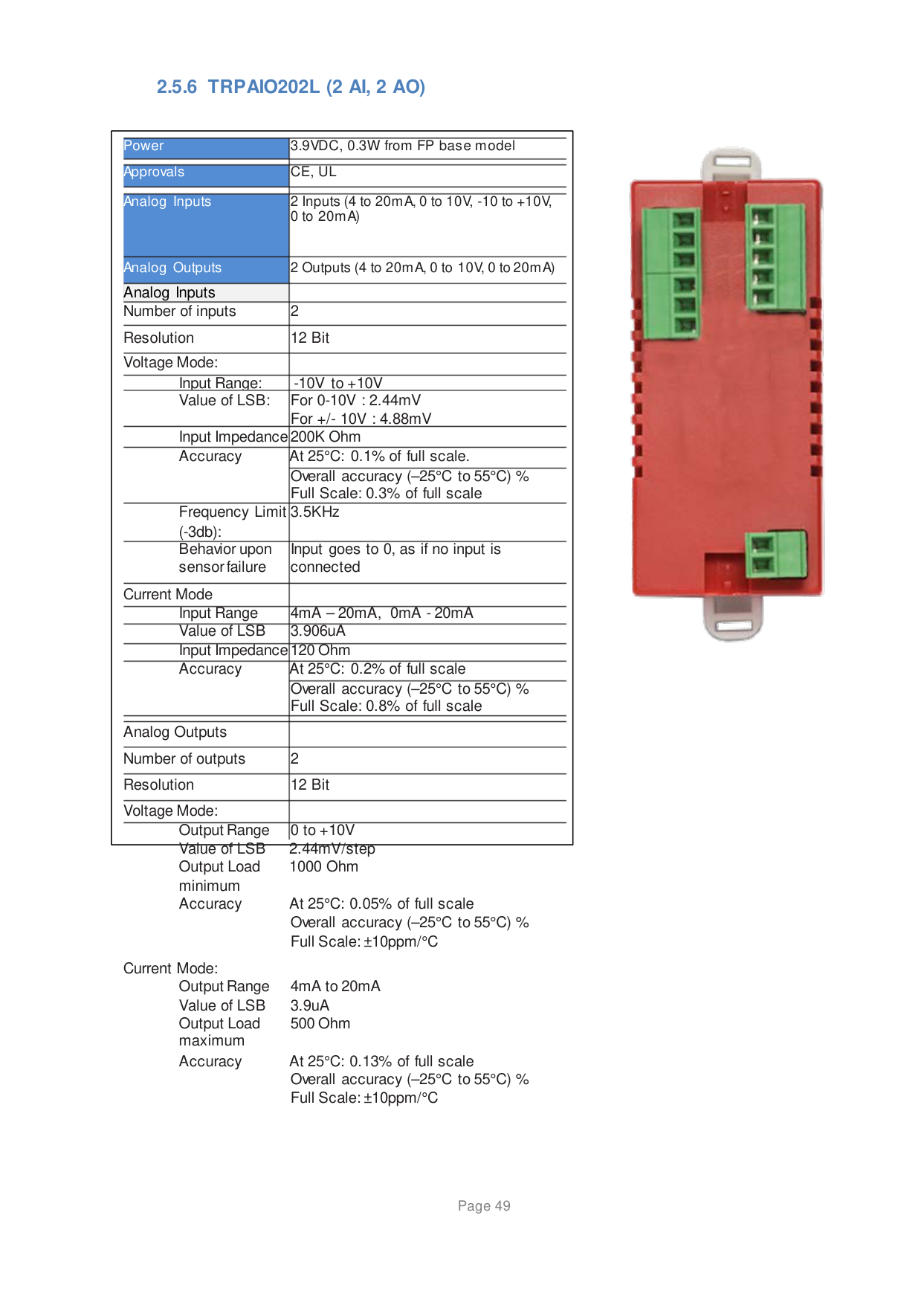
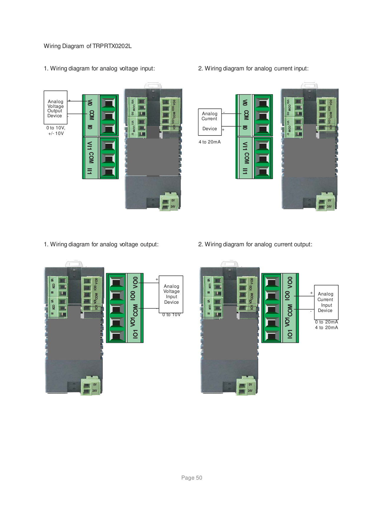
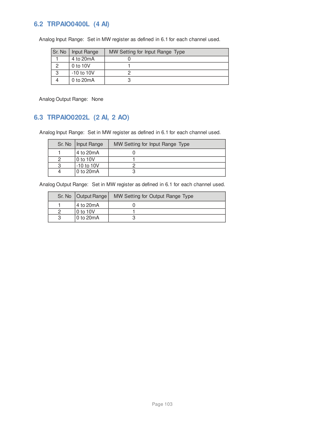
############## 2.5.6 TRPAIO202L (2 AI, 2 AO)
Power 3.9VDC, 0.3W from FP base model Approvals CE, UL Analog Inputs 2 Inputs (4 to 20mA, 0 to 10V, -10 to +10V,

0 to 20mA)
Analog Outputs 2 Outputs (4 to 20mA, 0 to 10V, 0 to 20mA) Analog Inputs Number of inputs 2 Resolution 12 Bit Voltage Mode:
Input Range: -10V to +10V Value of LSB: For 0-10V : 2.44mV
For +/- 10V : 4.88mV Input Impedance200K Ohm Accuracy At 25°C: 0.1% of full scale.
Overall accuracy (–25°C to 55°C) % Full Scale: 0.3% of full scale
Frequency Limit (-3db):
3.5KHz
Behavior upon sensor failure
Input goes to 0, as if no input is connected
Current Mode Input Range 4mA – 20mA, 0mA - 20mA Value of LSB 3.906uA Input Impedance120 Ohm Accuracy At 25°C: 0.2% of full scale
Overall accuracy (–25°C to 55°C) % Full Scale: 0.8% of full scale
Analog Outputs Number of outputs 2 Resolution 12 Bit Voltage Mode:
Output Range 0 to +10V Value of LSB 2.44mV/step Output Load minimum
1000 Ohm
Accuracy At 25°C: 0.05% of full scale Overall accuracy (–25°C to 55°C) % Full Scale: ±10ppm/°C
Current Mode: Output Range 4mA to 20mA Value of LSB 3.9uA Output Load maximum
500 Ohm
Accuracy At 25°C: 0.13% of full scale Overall accuracy (–25°C to 55°C) % Full Scale: ±10ppm/°C


Wiring Diagram of TRPRTX0202L
|Analog Voltage Output Device|+| | |---|---|---| |Analog Voltage Output Device|-| | |0 to 10V, +/- 10V|0 to 10V, +/- 10V| |


################## VI1II1


VI0COMII0 VI1COMII1
IO1VO1COMIO0VO0


0V 24V

| | | | | |---|---|---|---| |Analog Current
Device|-| | | |Analog Current
Device|+| | | |4 to 20mA|4 to 20mA| | |
| | |---| | |


VI1II1


VI0COMII0 VI1COMII1
IO1VO1COMIO0VO0


0V 24V


+


IO1IO0VO0


IO1IO0VO0
Analog Voltage Input Device


0 to 10V


0V 24V


IO1IO0VO0


IO1IO0VO0
+ Analog Current Input - Device


0 to 20mA 4 to 20mA


0V 24V

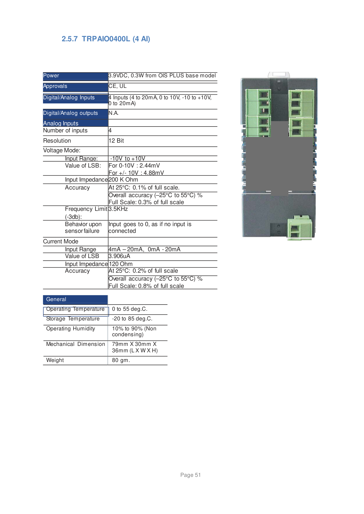
############## 2.5.7 TRPAIO0400L (4 AI)
|Power Approvals
|3.9VDC, 0.3W from OIS PLUS base model CE, UL| |---|---| |Digital/Analog Inputs
|4 Inputs (4 to 20mA, 0 to 10V, -10 to +10V, 0 to 20mA)| | |4 Inputs (4 to 20mA, 0 to 10V, -10 to +10V, 0 to 20mA)| |Digital/Analog outputs|N.A.| |Analog Inputs
| | |Number of inputs|4| |Resolution|12 Bit| |Voltage Mode:| | |Input Range:|-10V to +10V| |Value of LSB:|For 0-10V : 2.44mV For +/- 10V : 4.88mV| |Input Impedance|200 K Ohm| |Accuracy
|At 25°C: 0.1% of full scale.| |Accuracy
|Overall accuracy (–25°C to 55°C) % Full Scale: 0.3% of full scale| |Frequency Limit (-3db):|3.5KHz| |Behavior upon sensor failure|Input goes to 0, as if no input is connected| |Current Mode| | |Input Range|4mA – 20mA, 0mA - 20mA|
|Value of LSB|3.906uA| |Input Impedance|120 Ohm| |Accuracy
|At 25°C: 0.2% of full scale Overall accuracy (–25°C to 55°C) %| |Accuracy
|Full Scale: 0.8% of full scale|
|General
| | |---|---| |Operating Temperature|0 to 55 deg.C.| | |0 to 55 deg.C.| |Storage Temperature|-20 to 85 deg.C.| |Operating Humidity|10% to 90% (Non condensing)| |Mechanical Dimension|79mm X 30mm X 36mm (L X W X H)| |Weight|80 gm.|


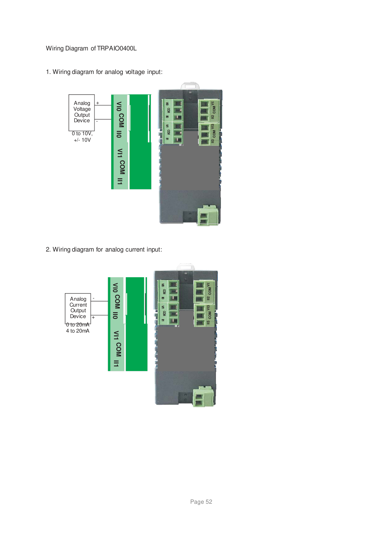
Wiring Diagram of TRPAIO0400L
0 to 10V, +/- 10V


+

Analog Voltage Output Device
II3COMVI3 II2COMVI2
################## VI0COMII0


################## VI1COMII1 VI0COMII0


II3COMVI3 II2COMVI2


+


0 to 20mA 4 to 20mA

VI1COMII1


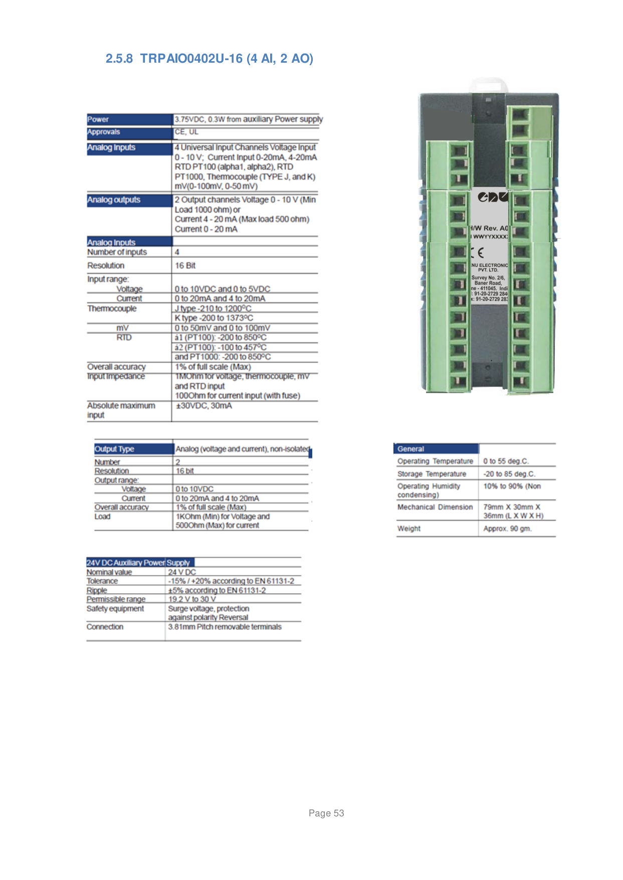
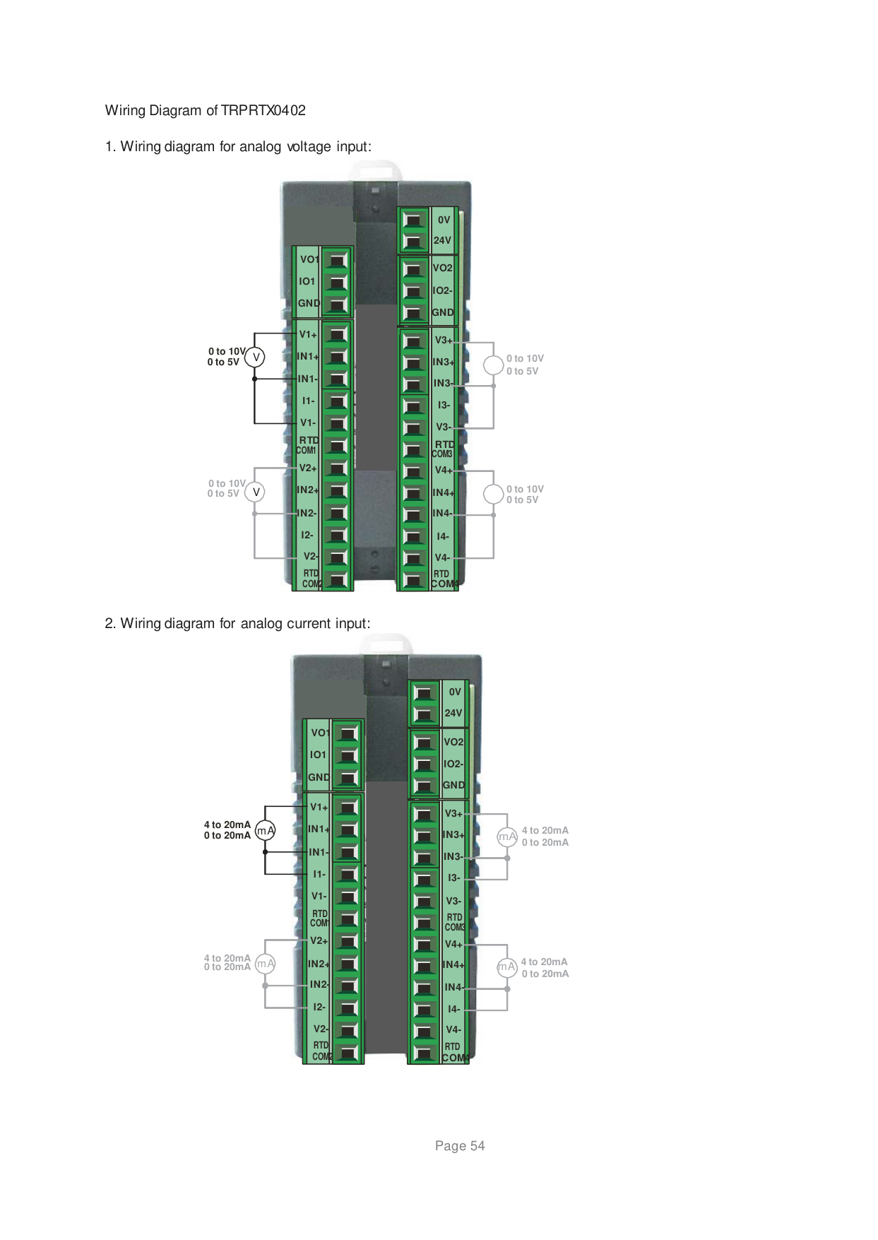
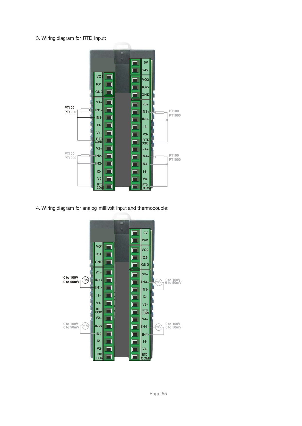
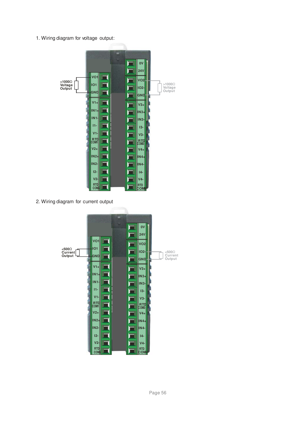
############## 2.5.8 TRPAIO0402U-16 (4 AI, 2 AO)


.


Wiring Diagram of TRPRTX0402
0 to 10V 0 to 5V
0 to 10V 0 to 5V
0 to 10V 0 to 5V
0 to 10V 0 to 5V

| |0V 24V| | |---|---|---| | |VO2 IO2GND| | |
|V3+
IN3+
IN3I3-
V3RTD
COM3
V4+ IN4+
IN4I4-
V4RTD
COM4| | |
|V3+
IN3+
IN3I3-
V3RTD
COM3
V4+ IN4+
IN4I4-
V4RTD
COM4| | | |V3+
IN3+
IN3I3-
V3RTD
COM3
V4+ IN4+
IN4I4-
V4RTD
COM4| | | |V3+
IN3+
IN3I3-
V3RTD
COM3
V4+ IN4+
IN4I4-
V4RTD
COM4| | | |V3+
IN3+
IN3I3-
V3RTD
COM3
V4+ IN4+
IN4I4-
V4RTD
COM4| | | |V3+
IN3+
IN3I3-
V3RTD
COM3
V4+ IN4+
IN4I4-
V4RTD
COM4| | | |V3+
IN3+
IN3I3-
V3RTD
COM3
V4+ IN4+
IN4I4-
V4RTD
COM4| |
| |VO1 IO1 GND| | |---|---|---| | |V1+
IN1+
IN1I1-
V1RTD
COM1
V2+ IN2+
IN2I2-
V2RTD COM2
|
| |V|V1+
IN1+
IN1I1-
V1RTD
COM1
V2+ IN2+
IN2I2-
V2RTD COM2
|
| | |V1+
IN1+
IN1I1-
V1RTD
COM1
V2+ IN2+
IN2I2-
V2RTD COM2
|
| | |V1+
IN1+
IN1I1-
V1RTD
COM1
V2+ IN2+
IN2I2-
V2RTD COM2
| | | |V1+
IN1+
IN1I1-
V1RTD
COM1
V2+ IN2+
IN2I2-
V2RTD COM2
| | |V|V1+
IN1+
IN1I1-
V1RTD
COM1
V2+ IN2+
IN2I2-
V2RTD COM2
| | | |V1+
IN1+
IN1I1-
V1RTD
COM1
V2+ IN2+
IN2I2-
V2RTD COM2
| | | |V1+
IN1+
IN1I1-
V1RTD
COM1
V2+ IN2+
IN2I2-
V2RTD COM2
| |


2U

| |0V 24V| | |---|---|---| | |VO2 IO2GND| | |
|V3+
IN3+
IN3I3-
V3RTD COM3 V4+ IN4+
IN4I4-
V4RTD
COM4| | |
|V3+
IN3+
IN3I3-
V3RTD COM3 V4+ IN4+
IN4I4-
V4RTD
COM4| | | |V3+
IN3+
IN3I3-
V3RTD COM3 V4+ IN4+
IN4I4-
V4RTD
COM4| | | |V3+
IN3+
IN3I3-
V3RTD COM3 V4+ IN4+
IN4I4-
V4RTD
COM4| | | |V3+
IN3+
IN3I3-
V3RTD COM3 V4+ IN4+
IN4I4-
V4RTD
COM4| | | |V3+
IN3+
IN3I3-
V3RTD COM3 V4+ IN4+
IN4I4-
V4RTD
COM4| |
| |VO1 IO1 GND| | |---|---|---| | |V1+
IN1+
IN1I1-
V1RTD COM1 V2+
IN2+
IN2I2-
V2RTD COM2
|
| | |V1+
IN1+
IN1I1-
V1RTD COM1 V2+
IN2+
IN2I2-
V2RTD COM2
|
| | |V1+
IN1+
IN1I1-
V1RTD COM1 V2+
IN2+
IN2I2-
V2RTD COM2
|
| | |V1+
IN1+
IN1I1-
V1RTD COM1 V2+
IN2+
IN2I2-
V2RTD COM2
| | | |V1+
IN1+
IN1I1-
V1RTD COM1 V2+
IN2+
IN2I2-
V2RTD COM2
| | | |V1+
IN1+
IN1I1-
V1RTD COM1 V2+
IN2+
IN2I2-
V2RTD COM2
| | | |V1+
IN1+
IN1I1-
V1RTD COM1 V2+
IN2+
IN2I2-
V2RTD COM2
| |


2U
4 to 20mA 0 to 20mA
mA 4 to 20mA 0 to 20mA

4 to 20mA
4 to 20mA
mA
0 to 20mA mA
0 to

PT100 PT1000
PT100 PT1000
PT100 PT1000
PT100 PT1000
COM2 COM4

| |0V 24V| | |---|---|---| | |VO2 IO2GND| | |
2U
|V3+
IN3+
IN3I3-
V3RTD
COM3
V4+ IN4+
IN4I4-
V4RTD
| | |
2U
|V3+
IN3+
IN3I3-
V3RTD
COM3
V4+ IN4+
IN4I4-
V4RTD
| | | |V3+
IN3+
IN3I3-
V3RTD
COM3
V4+ IN4+
IN4I4-
V4RTD
| | | |V3+
IN3+
IN3I3-
V3RTD
COM3
V4+ IN4+
IN4I4-
V4RTD
| | | |V3+
IN3+
IN3I3-
V3RTD
COM3
V4+ IN4+
IN4I4-
V4RTD
| |
| |V3+
IN3+
IN3I3-
V3RTD
COM3
V4+ IN4+
IN4I4-
V4RTD
| |
| |VO1 IO1 GND| | |---|---|---| | |V1+
IN1+
IN1I1-
V1RTD
COM1
V2+ IN2+
IN2I2-
V2RTD
|
| | |V1+
IN1+
IN1I1-
V1RTD
COM1
V2+ IN2+
IN2I2-
V2RTD
|
| | |V1+
IN1+
IN1I1-
V1RTD
COM1
V2+ IN2+
IN2I2-
V2RTD
|
| | |V1+
IN1+
IN1I1-
V1RTD
COM1
V2+ IN2+
IN2I2-
V2RTD
| | | |V1+
IN1+
IN1I1-
V1RTD
COM1
V2+ IN2+
IN2I2-
V2RTD
| | | |V1+
IN1+
IN1I1-
V1RTD
COM1
V2+ IN2+
IN2I2-
V2RTD
| | | |V1+
IN1+
IN1I1-
V1RTD
COM1
V2+ IN2+
IN2I2-
V2RTD
| |


| |0V 24V|mV| |---|---|---| | |VO2 IO2GND|mV| |
|V3+
IN3+
IN3I3-
V3RTD COM3 V4+
IN4+
IN4I4-
V4RTD
COM4|mV| |
|V3+
IN3+
IN3I3-
V3RTD COM3 V4+
IN4+
IN4I4-
V4RTD
COM4| | | |V3+
IN3+
IN3I3-
V3RTD COM3 V4+
IN4+
IN4I4-
V4RTD
COM4|mV| | |V3+
IN3+
IN3I3-
V3RTD COM3 V4+
IN4+
IN4I4-
V4RTD
COM4| | | |V3+
IN3+
IN3I3-
V3RTD COM3 V4+
IN4+
IN4I4-
V4RTD
COM4| |
|
|VO1 IO1 GND| | |---|---|---| |
|V1+
IN1+
IN1I1-
V1RTD COM1 V2+
IN2+
IN2I2-
V2RTD COM2
|
| | |V1+
IN1+
IN1I1-
V1RTD COM1 V2+
IN2+
IN2I2-
V2RTD COM2
|
| |mV|V1+
IN1+
IN1I1-
V1RTD COM1 V2+
IN2+
IN2I2-
V2RTD COM2
|
| |mV|V1+
IN1+
IN1I1-
V1RTD COM1 V2+
IN2+
IN2I2-
V2RTD COM2
| | | |V1+
IN1+
IN1I1-
V1RTD COM1 V2+
IN2+
IN2I2-
V2RTD COM2
| |

| |V1+
IN1+
IN1I1-
V1RTD COM1 V2+
IN2+
IN2I2-
V2RTD COM2
| |


2U
0 to 100V 0 to 50mV
0 to 100V 0 to 50mV
0 to 100V 0 to 50mV 0 to 50mV
0 to 100V
0V
>1000Ω Voltage Output
VO1 IO1 GND
24V
VO2 IO2GND
>1000Ω Voltage Output
V1+
V1RTD
COM1 V2+ IN2+
V3+
V3RTD
COM3
V4+ IN4+
V2RTD COM2
V4RTD
COM4


2U

| |0V 24V| | | |---|---|---|---| | |VO2 IO2GND| | | | |VO2 IO2GND| | | |
2U
|V3+
IN3+
IN3I3-
V3RTD
COM3
V4+ IN4+
IN4I4-
V4RTD
COM4| | | | |V3+
IN3+
IN3I3-
V3RTD
COM3
V4+ IN4+
IN4I4-
V4RTD
COM4| | |
| | |VO1 IO1 GND| | |---|---|---|---| | | |VO1 IO1 GND| | | | |VO1 IO1 GND| | | | |V1+
IN1+
IN1I1-
V1RTD
COM1 V2+ IN2+
IN2I2-
V2RTD COM2
|
| | | |V1+
IN1+
IN1I1-
V1RTD
COM1 V2+ IN2+
IN2I2-
V2RTD COM2
| |
<500Ω Current Output
<500Ω Current Output


PEA040

############# 2.6 Installation Instructions
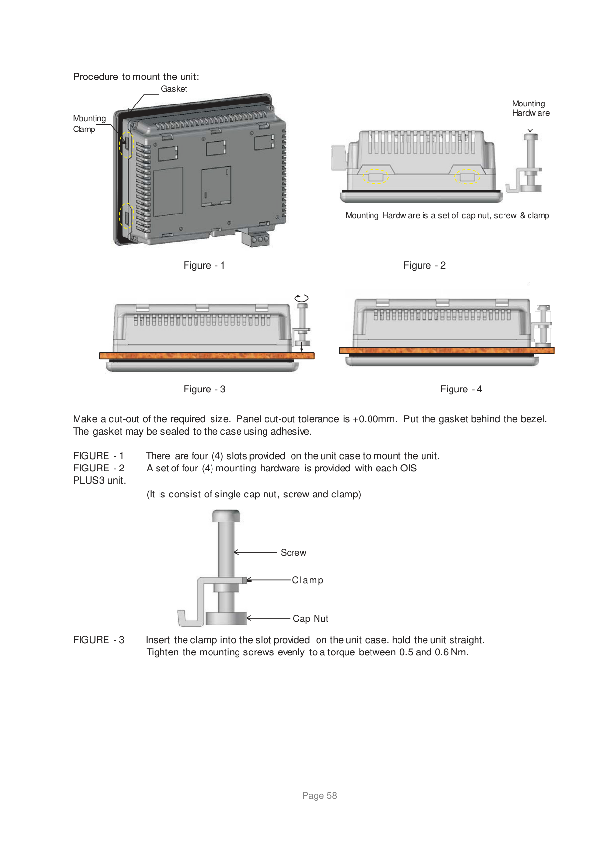
The OIS PLUS should be mounted on a panel. A sealing gasket and mounting clamps are provided with each OIS PLUS unit for proper installation.
Environmental Considerations: Make sure that the unit is installed correctly and that the operating limits are followed (see Specifications for OIS PLUS). Do not operate the OIS PLUS in areas subject to explosion hazards due to flammable gases, vapors or dusts. A OIS PLUS should not be installed where fast temperature variations are present. Highly humid areas are also to be avoided. High humidity causes condensation of water in the unit.
Location Considerations: Care should be taken when locating equipment behind the OIS PLUS to ensure that AC power wiring, PLC output modules, contactors, starters, relays and any other source of electrical interference are located away from the OIS PLUS. Particular care should be taken to locate variable speed drives and switching power supplies away from the OIS PLUS.
Panel Mounting This section presents the dimensional sketches and panel cutouts for OIS PLUS models. (All dimensions are in mm and drawings are not to scale.)
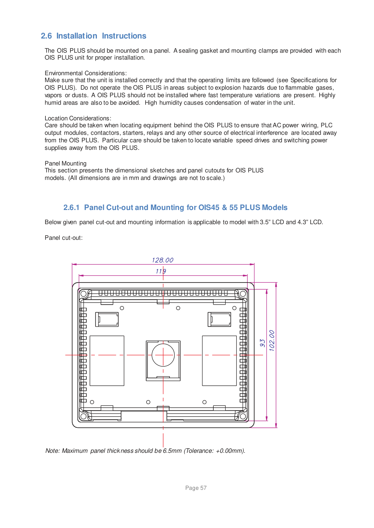
############## 2.6.1 Panel Cut-out and Mounting for OIS45 & 55 PLUS Models
Below given panel cut-out and mounting information is applicable to model with 3.5” LCD and 4.3” LCD.
Panel cut-out:
| | | |---|---| | | |
| | | |---|---|
| | | |---|---|
Note: Maximum panel thickness should be 6.5mm (Tolerance: +0.00mm).
Procedure to mount the unit:
Gasket

Mounting Clamp
Mounting Hardw are


Mounting Hardw are is a set of cap nut, screw & clamp
Figure - 1 Figure - 2

|| |---|


|| |---|
Figure - 3 Figure - 4
Make a cut-out of the required size. Panel cut-out tolerance is +0.00mm. Put the gasket behind the bezel. The gasket may be sealed to the case using adhesive.
(It is consist of single cap nut, screw and clamp)
Screw
Clamp
Cap Nut

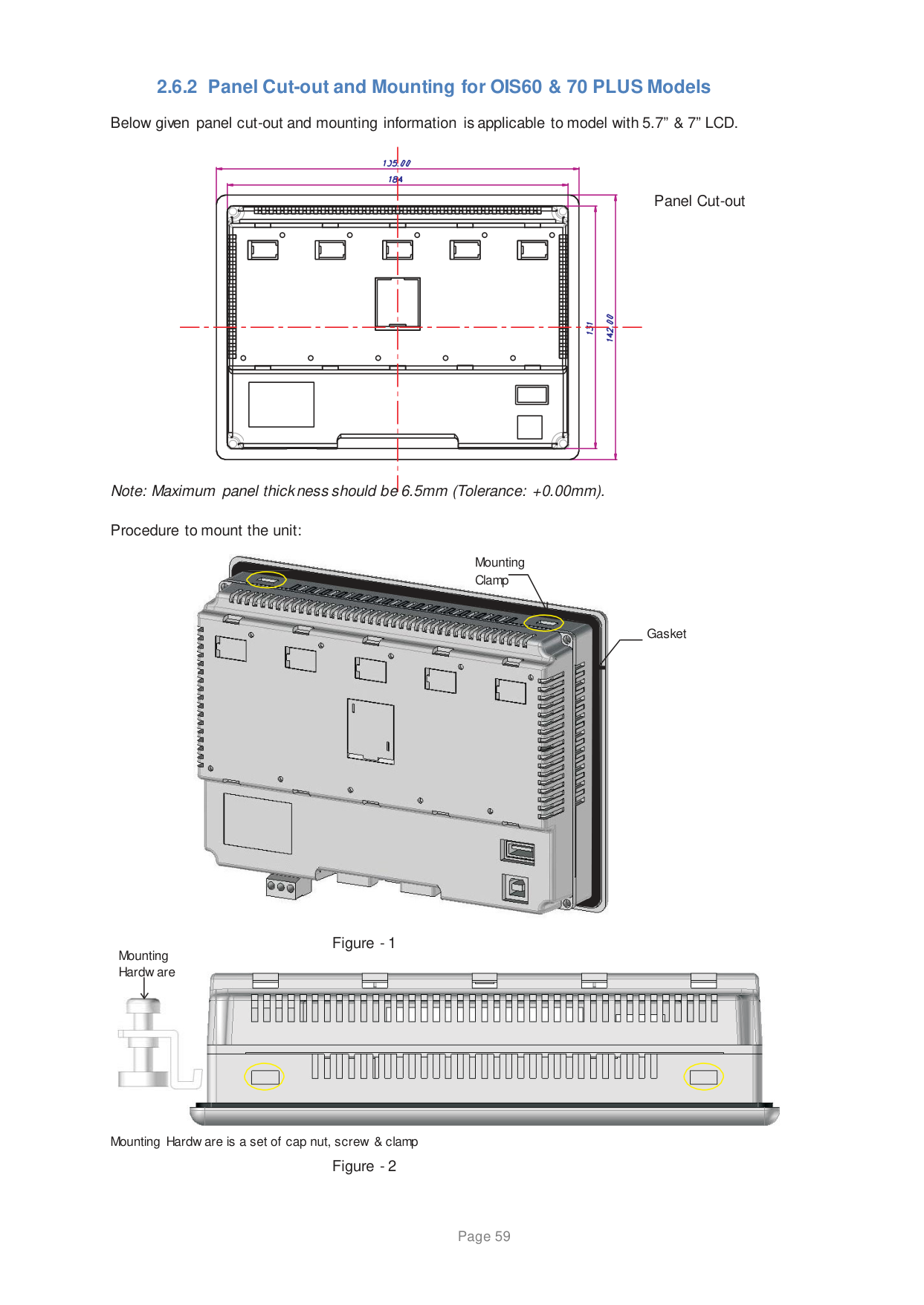
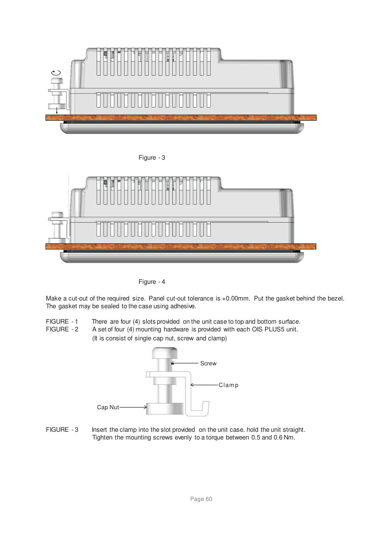
############## 2.6.2 Panel Cut-out and Mounting for OIS60 & 70 PLUS Models
Below given panel cut-out and mounting information is applicable to model with 5.7” & 7” LCD.


| | | |---|---| | | |
| | | | |---|---|---| | | | |


| | | |---|---| | | |
Panel Cut-out

Note: Maximum panel thickness should be 6.5mm (Tolerance: +0.00mm).
Procedure to mount the unit:
Mounting Clamp

Gasket
Mounting Hardw are is a set of cap nut, screw & clamp
Mounting Hardw are


Page 59

|| |---|


|| |---|
Make a cut-out of the required size. Panel cut-out tolerance is +0.00mm. Put the gasket behind the bezel. The gasket may be sealed to the case using adhesive.
Screw
Clamp
Cap Nut

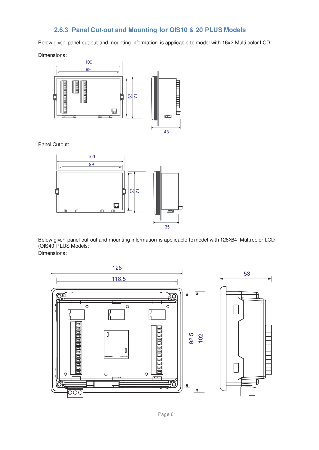
2.6.3 Panel Cut-out and Mounting for OIS10 & 20 PLUS Models Below given panel cut-out and mounting information is applicable to model with 16x2 Multi color LCD. Dimensions:
109 99

| | | |---|---| | | | | | | | | | | | | | | | | | | | | | | | | | | | | | | | | | | | | | | | | | | | | | | | |

43
################### Panel Cutout:
109 99

35
Below given panel cut-out and mounting information is applicable to model with 128X64 Multi color LCD (OIS40 PLUS Models: Dimensions:
128
53 118.5
| | | | | | | | | |---|---|---|---|---|---|---|---| || | |---| || | |---| || | |---| || | |---| || | |---| || | |---| || | |---| || | |---| | | | | | | | | | | | | | | | | | | | | | | | | | | | |

############## 2.6.4 Mounting for Clip-on I/O Modules
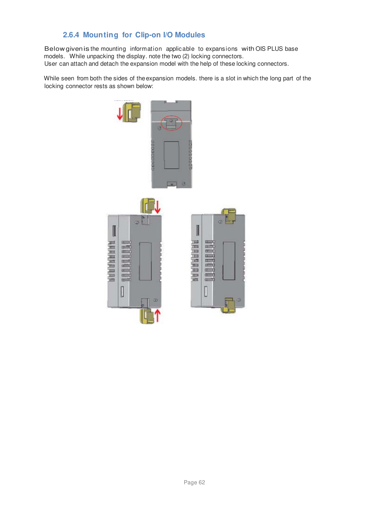
Below given isthe mounting information applicable to expansions with OIS PLUS base models. While unpacking the display. note the two (2) locking connectors. User can attach and detach the expansion model with the help of these locking connectors.
While seen from both the sides of the expansion models. there is a slot in which the long part of the locking connector rests as shown below:


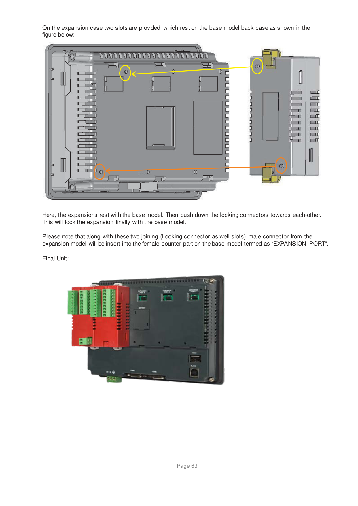
On the expansion case two slots are provided which rest on the base model back case as shown in the figure below:


Here, the expansions rest with the base model. Then push down the locking connectors towards each-other. This will lock the expansion finally with the base model.
Please note that along with these two joining (Locking connector as well slots), male connector from the expansion model will be insert into the female counter part on the base model termed as “EXPANSION PORT”.
Final Unit:


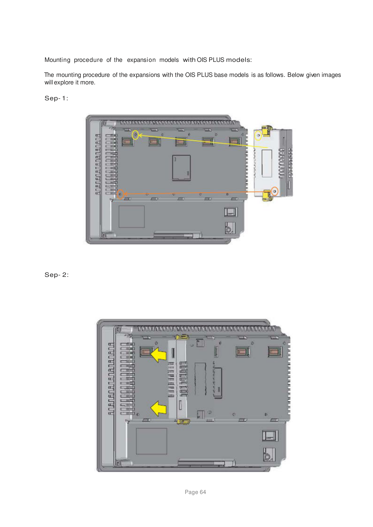
Mounting procedure of the expansion models with OIS PLUS models:
The mounting procedure of the expansions with the OIS PLUS base models is as follows. Below given images will explore it more.


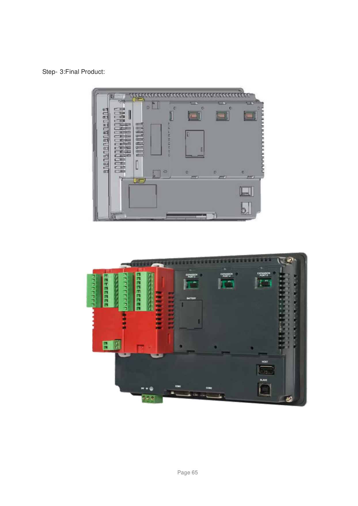
################# Step- 3:Final Product:


############# 2.7 Power Supply Wiring Diagram
If wiring is to be exposed to lightening or other electrical surges, use appropriate surge suppression devices. Keep AC, high energy and rapidly switching DC wiring separate from signal wires.
Connecting high voltages or AC power mains to the DC input will make unit unusable and may create an
electrical shock hazard to personnel. Such a failure or shock could result in serious personal injury, loss of life and/or equipment damage. DC voltage sources should provide proper isolation from main AC power and similar hazards.
Pin description of the power connector for all OIS PLUS models is as follows:

DC- EARTH
DC+ 24VDC
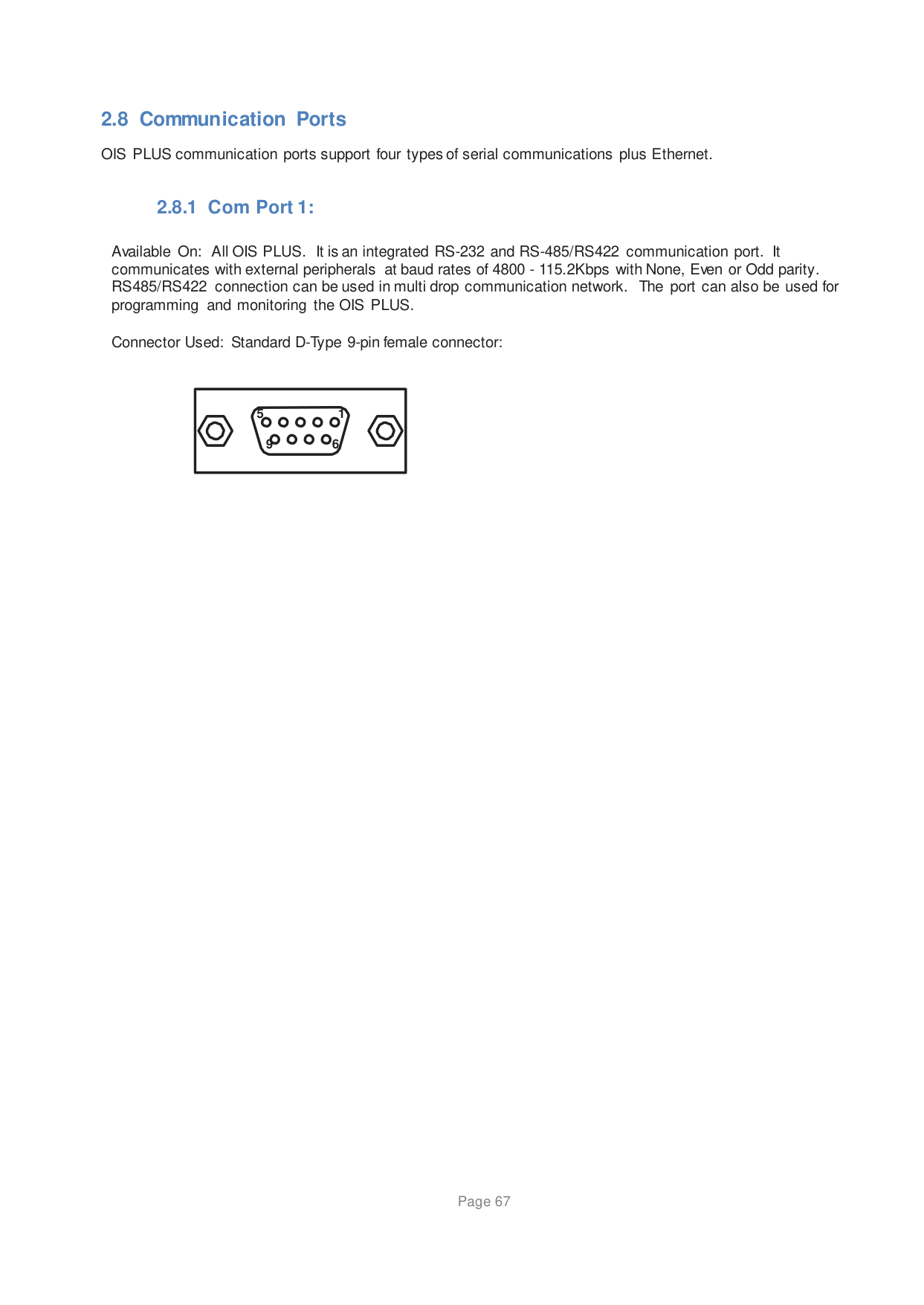
############## 2.8.1 Com Port 1:
Available On: All OIS PLUS. It is an integrated RS-232 and RS-485/RS422 communication port. It communicates with external peripherals at baud rates of 4800 - 115.2Kbps with None, Even or Odd parity. RS485/RS422 connection can be used in multi drop communication network. The port can also be used for programming and monitoring the OIS PLUS.
Connector Used: Standard D-Type 9-pin female connector:
|5 1 9 6| |---|
|Pin number|Name|Description| |---|---|---| |1|TX+|RS485 transmit +| |2|TXD|RS232 transmit| |3|RXD|RS232 receive| |4|RX+|RS485 receive +| |5|GND|Ground| |6|NC|No connection| |7|NC|No connection| |8|TX-|RS485 transmit -| |9|RX-|RS485 receive -|
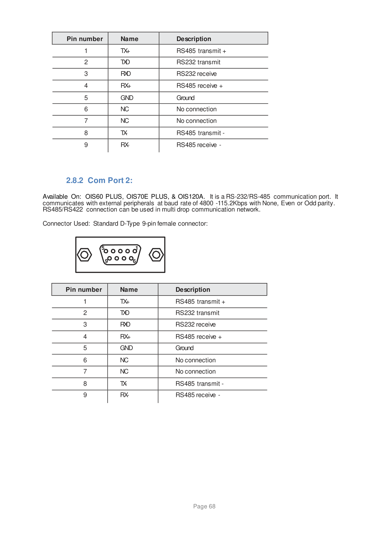
############## 2.8.2 Com Port 2:
Available On: OIS60 PLUS, OIS70E PLUS, & OIS120A. It is a RS-232/RS-485 communication port. It communicates with external peripherals at baud rate of 4800 -115.2Kbps with None, Even or Odd parity. RS485/RS422 connection can be used in multi drop communication network.
Connector Used: Standard D-Type 9-pin female connector:
|5 1
9 6| |---|
|Pin number|Name|Description| |---|---|---| |1|TX+|RS485 transmit +| |2|TXD|RS232 transmit|
|3|RXD|RS232 receive| |4|RX+|RS485 receive +| |5|GND|Ground| |6|NC|No connection| |7|NC|No connection| |8|TX-|RS485 transmit -| |9|RX-|RS485 receive -|
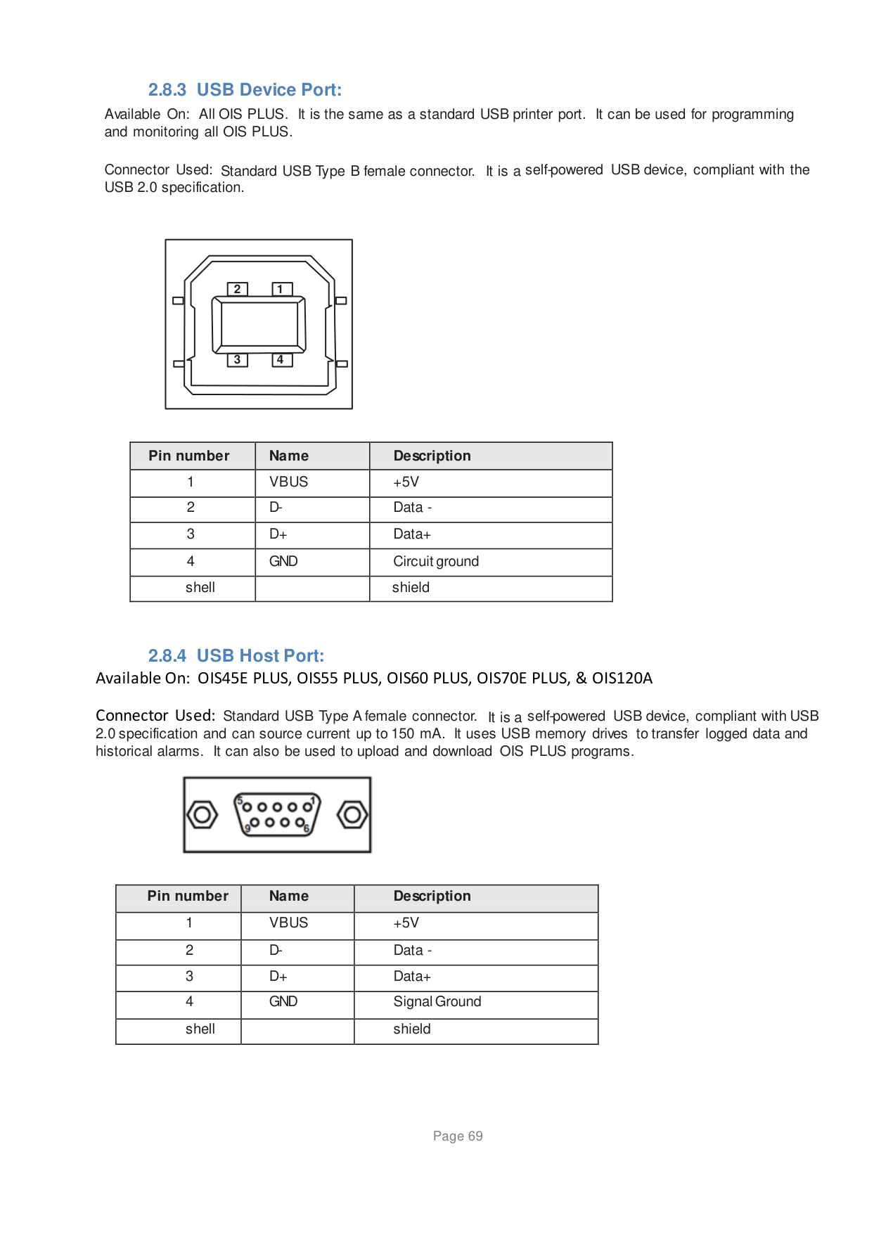
############## 2.8.3 USB Device Port:
Available On: All OIS PLUS. It is the same as a standard USB printer port. It can be used for programming and monitoring all OIS PLUS.
Connector Used: Standard USB Type B female connector. It is a self-powered USB device, compliant with the USB 2.0 specification.
|2 1
3 4
| |---|
|Pin number|Name|Description| |---|---|---| |1|VBUS|+5V| |2|D-|Data -| |3|D+|Data+| |4|GND|Circuit ground| |shell| |shield|
2.8.4 USB Host Port: Available On: OIS45E PLUS, OIS55 PLUS, OIS60 PLUS, OIS70E PLUS, & OIS120A Connector Used: Standard USB Type A female connector. It is a self-powered USB device, compliant with USB


|Pin number|Name|Description| |---|---|---| |1|VBUS|+5V| |2|D-|Data -| |3|D+|Data+| |4|GND|Signal Ground| |shell| |shield|
############## 2.8.5 Ethernet Port:
Refer to Ethernet User’s Manual, UM-OISPLUS-E003
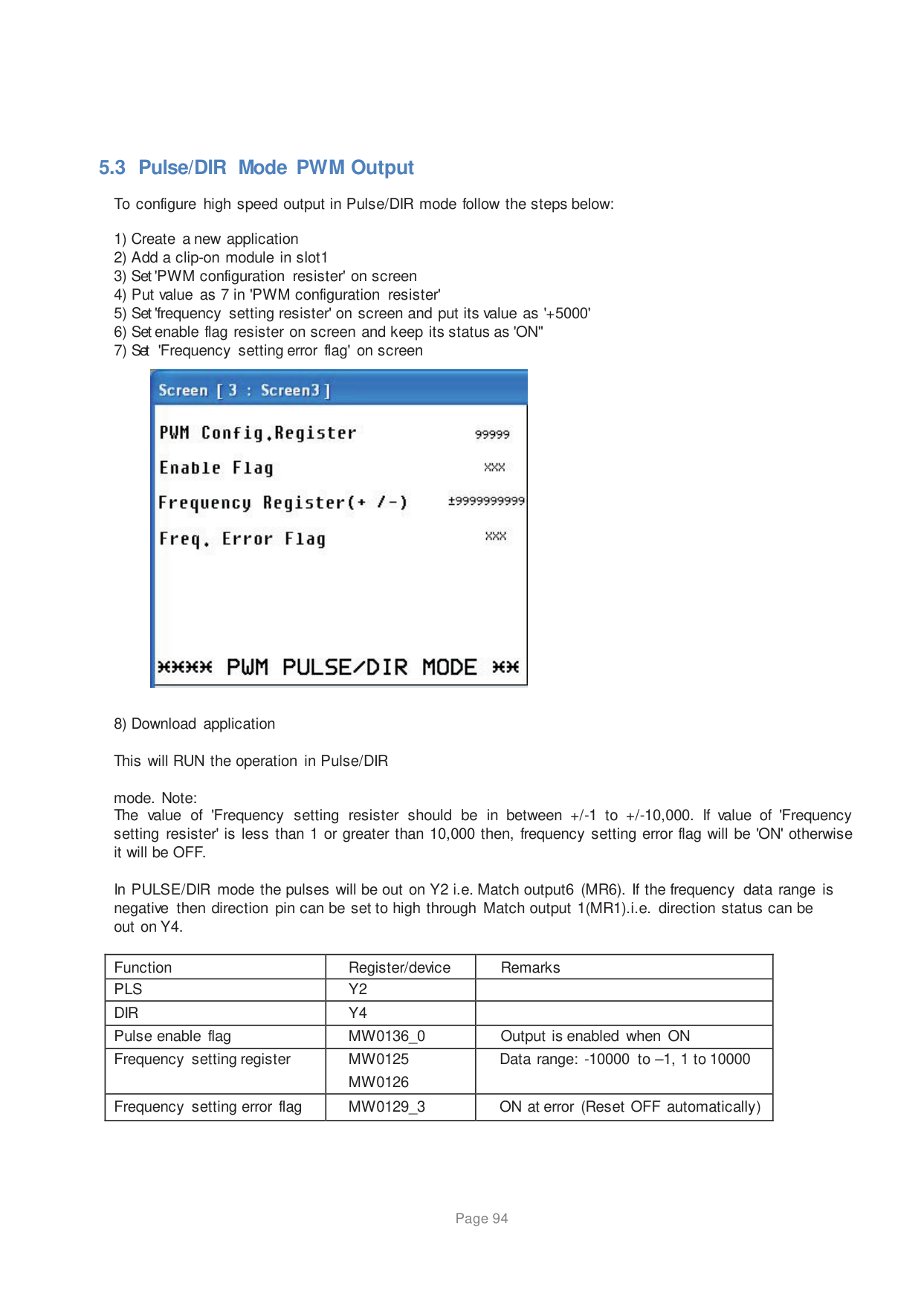
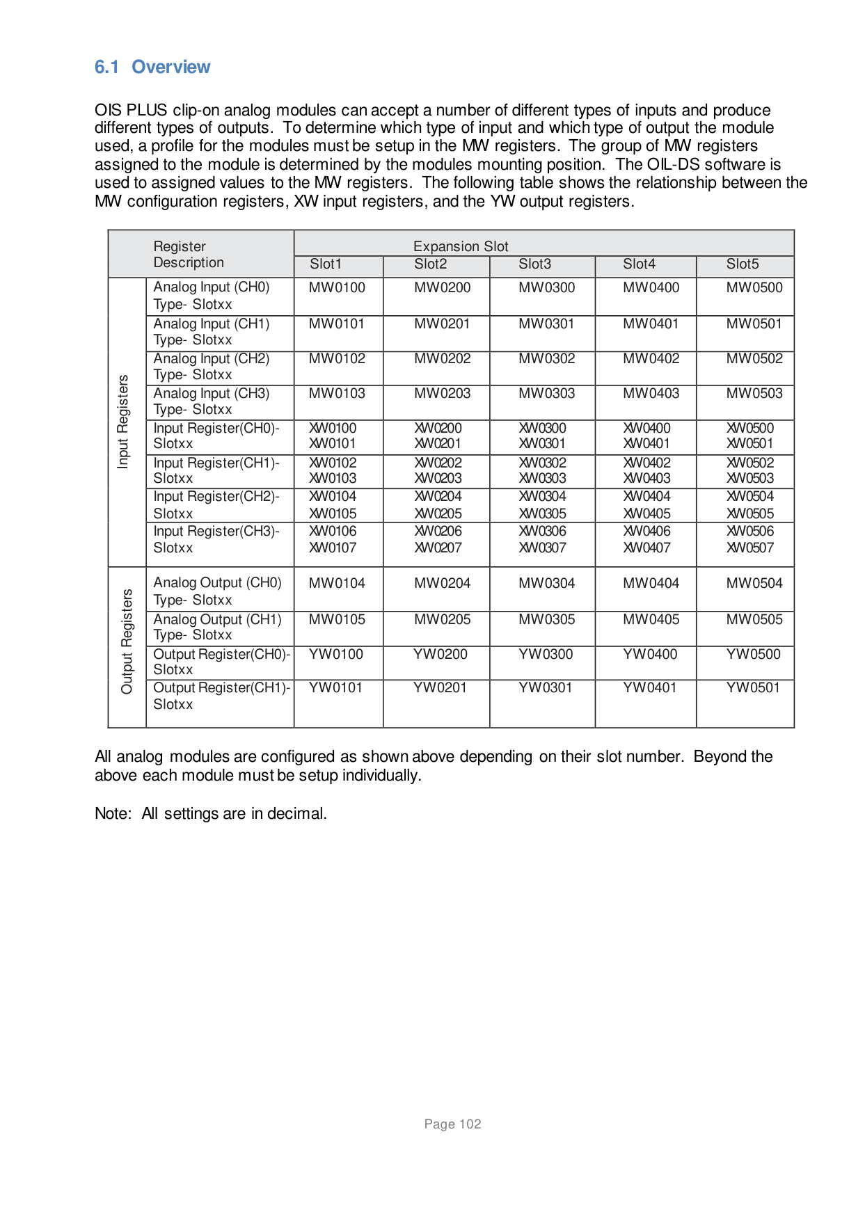
######### BASIC I/O ALLOCATION & SETUP
♦ I/O Allocation
♦ Setup Registers
Different OIS PLUS displays have different types of I/O.
No I/O: OIS12, OIS22, OIS40 PLUS, & OIS120A Fixed I/O: OIS10 PLUS & OIS20 PLUS Clip-on I/O: OIS40E PLUS, OIS55 PLUS, OIS60 PLUS, & OIS70E PLUS
Three types of registers are associated with the I/O
XW: Input Registers YW: Output Registers MW: Setup Registers
############# 3.1 I/O Allocation
For fixed I/O OIS, the allocation is done when the display is selected. For OIS with clip-on modules, the I/O allocation is done when the module is selected. Each register contains 16 bits. The bits are addressed as follows
1st Input Register XW0000 Inputs X0000 to X0015 1st Output Register YW0000 Outputs Y0000 to Y0015
For Clip-on I/O the module will be assigned XW registers, YW registers, or a combination of XW & YW registers depending on the module type.
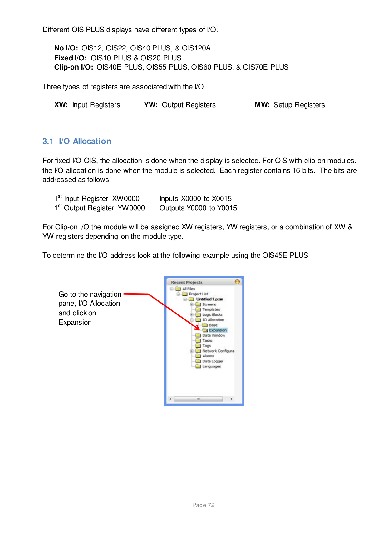
To determine the I/O address look at the following example using the OIS45E PLUS


Go to the navigation pane, I/O Allocation and click on Expansion

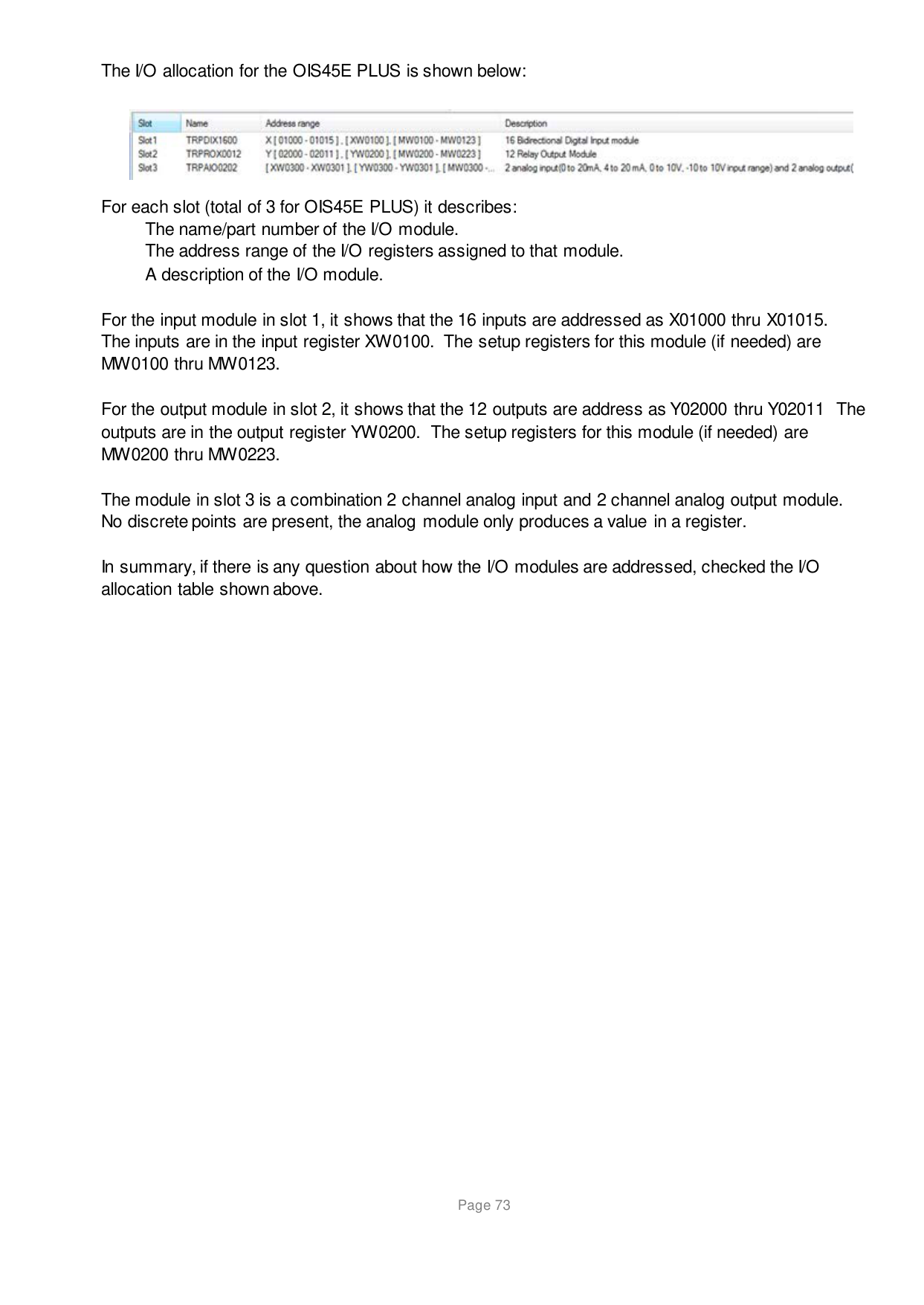
The I/O allocation for the OIS45E PLUS is shown below:


For each slot (total of 3 for OIS45E PLUS) it describes: The name/part number of the I/O module. The address range of the I/O registers assigned to that module. A description of the I/O module.
For the input module in slot 1, it shows that the 16 inputs are addressed as X01000 thru X01015. The inputs are in the input register XW0100. The setup registers for this module (if needed) are MW0100 thru MW0123.
For the output module in slot 2, it shows that the 12 outputs are address as Y02000 thru Y02011 The outputs are in the output register YW0200. The setup registers for this module (if needed) are MW0200 thru MW0223.
The module in slot 3 is a combination 2 channel analog input and 2 channel analog output module. No discrete points are present, the analog module only produces a value in a register.
In summary, if there is any question about how the I/O modules are addressed, checked the I/O allocation table shown above.
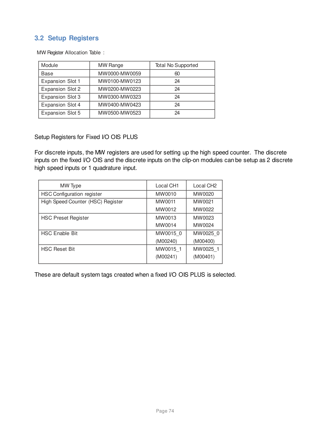
############# 3.2 Setup Registers
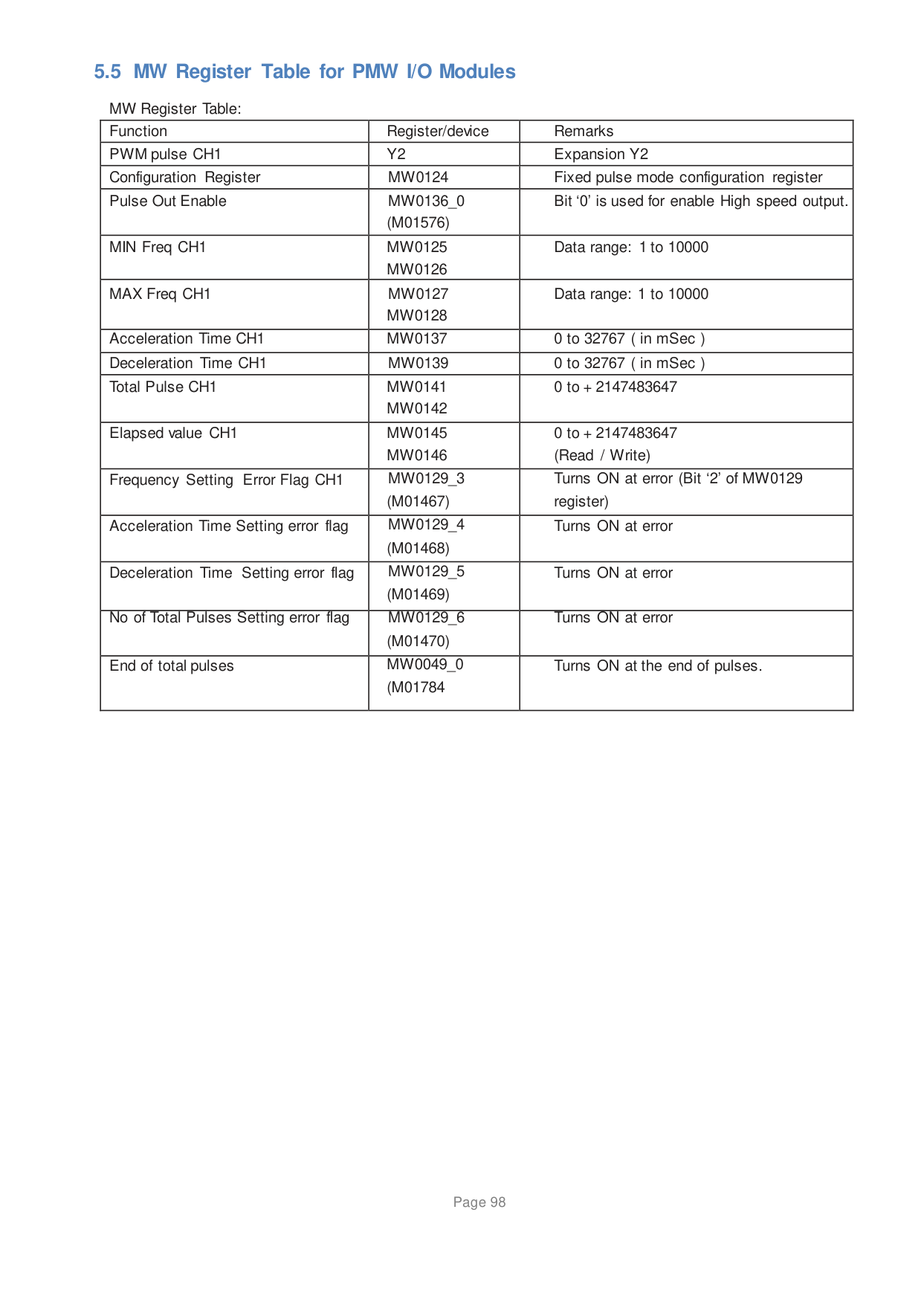
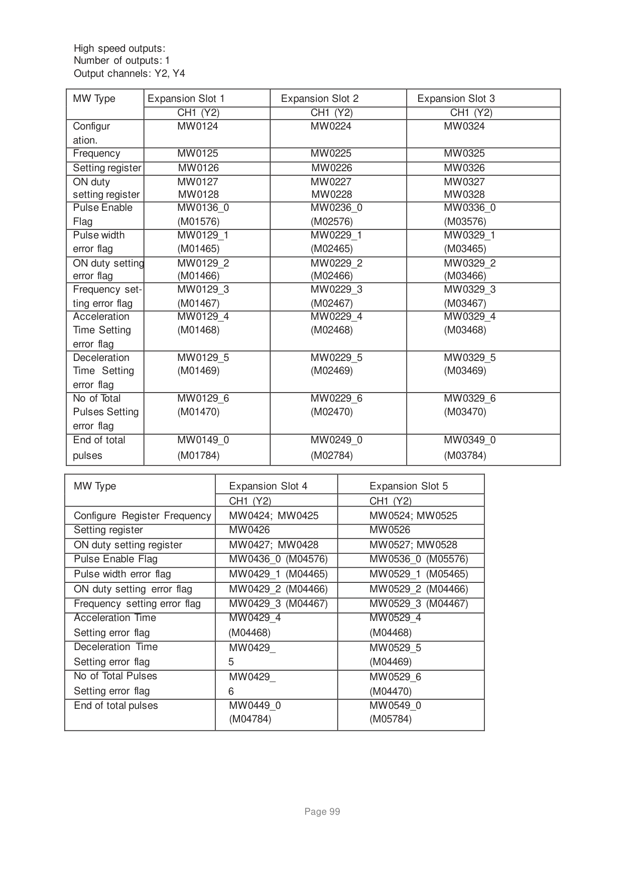
MW Register Allocation Table :
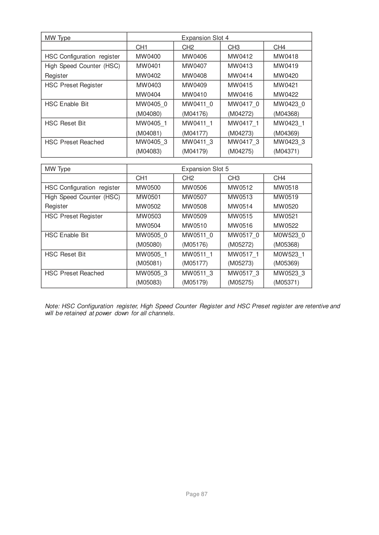
|Module|MW Range|Total No Supported| |---|---|---| |Base|MW0000-MW0059|60| |Expansion Slot 1|MW0100-MW0123|24| |Expansion Slot 2|MW0200-MW0223|24| |Expansion Slot 3|MW0300-MW0323|24| |Expansion Slot 4|MW0400-MW0423|24| |Expansion Slot 5|MW0500-MW0523|24|
Setup Registers for Fixed I/O OIS PLUS
For discrete inputs, the MW registers are used for setting up the high speed counter. The discrete inputs on the fixed I/O OIS and the discrete inputs on the clip-on modules can be setup as 2 discrete high speed inputs or 1 quadrature input.
|MW Type|Local CH1|Local CH2| |---|---|---| |HSC Configuration register|MW0010|MW0020| |High Speed Counter (HSC) Register|MW0011
MW0012
|MW0021
MW0022
| |HSC Preset Register|MW0013
MW0014
|MW0023
MW0024
| |HSC Enable Bit|MW0015_0 (M00240)|MW0025_0 (M00400)| |HSC Reset Bit|MW0015_1 (M00241)|MW0025_1 (M00401)|
These are default system tags created when a fixed I/O OIS PLUS is selected.
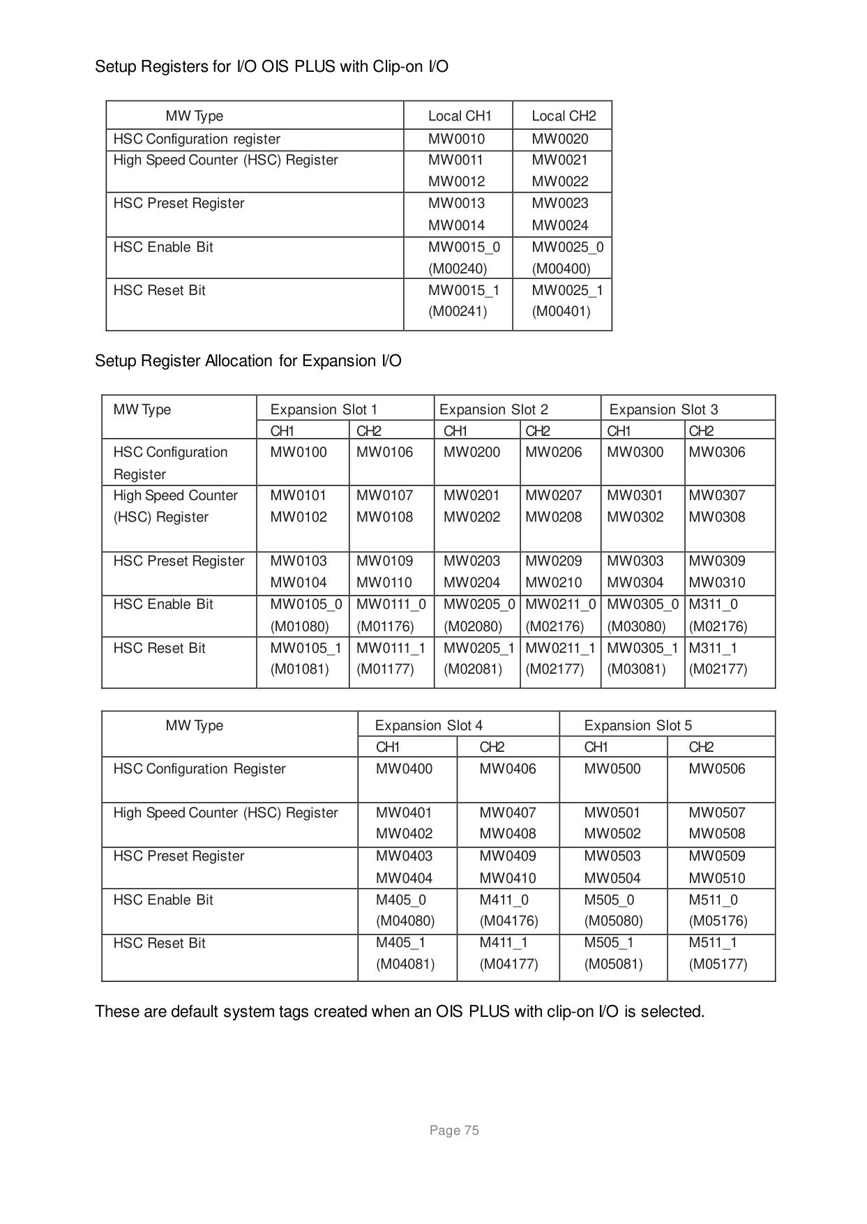
Setup Registers for I/O OIS PLUS with Clip-on I/O
|MW Type|Local CH1|Local CH2| |---|---|---| |HSC Configuration register|MW0010|MW0020| |High Speed Counter (HSC) Register|MW0011
MW0012
|MW0021
MW0022
| |HSC Preset Register|MW0013
MW0014
|MW0023
MW0024
| |HSC Enable Bit|MW0015_0 (M00240)|MW0025_0 (M00400)| |HSC Reset Bit|MW0015_1 (M00241)|MW0025_1 (M00401)|
Setup Register Allocation for Expansion I/O
|MW Type|Expansion Slot 1|Expansion Slot 1|Expansion Slot 2|Expansion Slot 2|Expansion Slot 3|Expansion Slot 3| |---|---|---|---|---|---|---| |MW Type|CH1|CH2|CH1|CH2|CH1|CH2| |HSC Configuration Register|MW0100|MW0106|MW0200|MW0206|MW0300|MW0306| |High Speed Counter (HSC) Register|MW0101
MW0102
|MW0107
MW0108
|MW0201
MW0202
|MW0207
MW0208
|MW0301
MW0302
|MW0307
MW0308
| |HSC Preset Register|MW0103
MW0104
|MW0109
MW0110
|MW0203
MW0204
|MW0209
MW0210
|MW0303
MW0304
|MW0309
MW0310
| |HSC Enable Bit|MW0105_0 (M01080)|MW0111_0 (M01176)|MW0205_0 (M02080)|MW0211_0 (M02176)|MW0305_0 (M03080)|M311_0 (M02176)| |HSC Reset Bit|MW0105_1 (M01081)|MW0111_1 (M01177)|MW0205_1 (M02081)|MW0211_1 (M02177)|MW0305_1 (M03081)|M311_1 (M02177)|
|MW Type
|Expansion Slot 4|Expansion Slot 4|Expansion Slot 5|Expansion Slot 5| |---|---|---|---|---| |MW Type
|CH1|CH2|CH1|CH2| |HSC Configuration Register|MW0400|MW0406|MW0500|MW0506| |High Speed Counter (HSC) Register|MW0401
MW0402
|MW0407
MW0408
|MW0501
MW0502
|MW0507
MW0508
| |HSC Preset Register|MW0403
MW0404
|MW0409
MW0410
|MW0503
MW0504
|MW0509
MW0510
| |HSC Enable Bit|M405_0 (M04080)|M411_0 (M04176)|M505_0 (M05080)|M511_0 (M05176)| |HSC Reset Bit|M405_1 (M04081)|M411_1 (M04177)|M505_1 (M05081)|M511_1 (M05177)|
These are default system tags created when an OIS PLUS with clip-on I/O is selected.
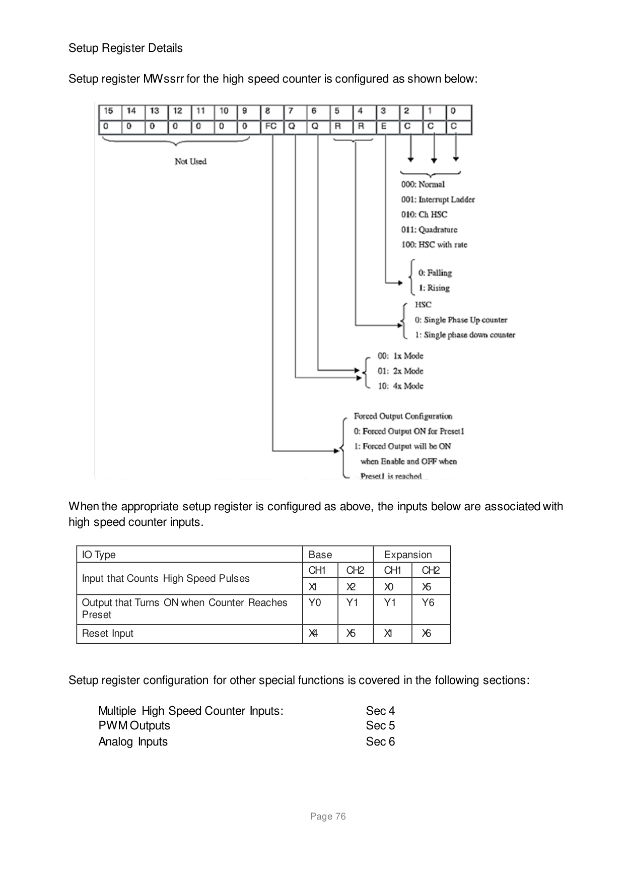
Setup Register Details
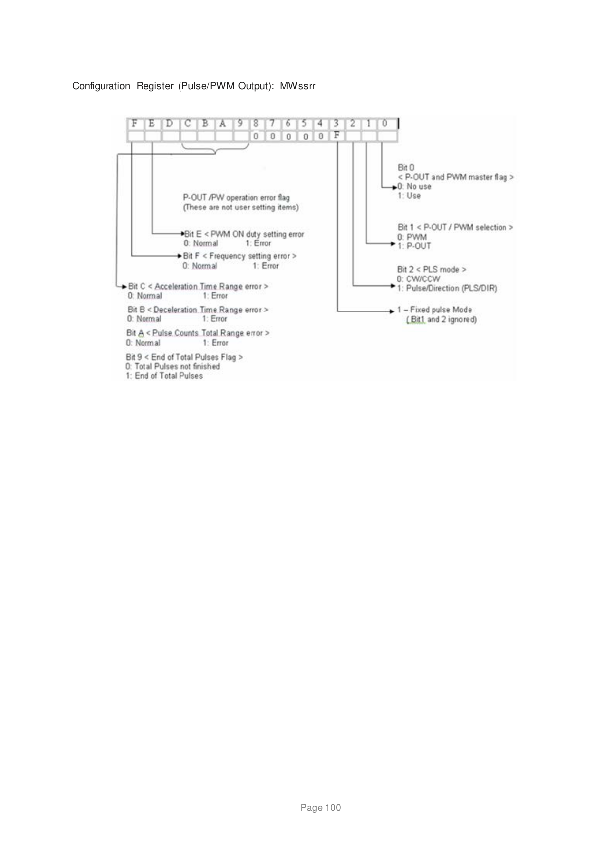
Setup register MWssrr for the high speed counter is configured as shown below:


When the appropriate setup register is configured as above, the inputs below are associated with high speed counter inputs.
|IO Type|Base|Base|Expansion|Expansion| |---|---|---|---|---| |Input that Counts High Speed Pulses|CH1|CH2|CH1|CH2| |Input that Counts High Speed Pulses|X1|X2|X0|X5| |Output that Turns ON when Counter Reaches Preset|Y0|Y1|Y1|Y6| |Reset Input|X4|X5|X1|X6|
Setup register configuration for other special functions is covered in the following sections:
Multiple High Speed Counter Inputs: Sec 4 PWM Outputs Sec 5 Analog Inputs Sec 6
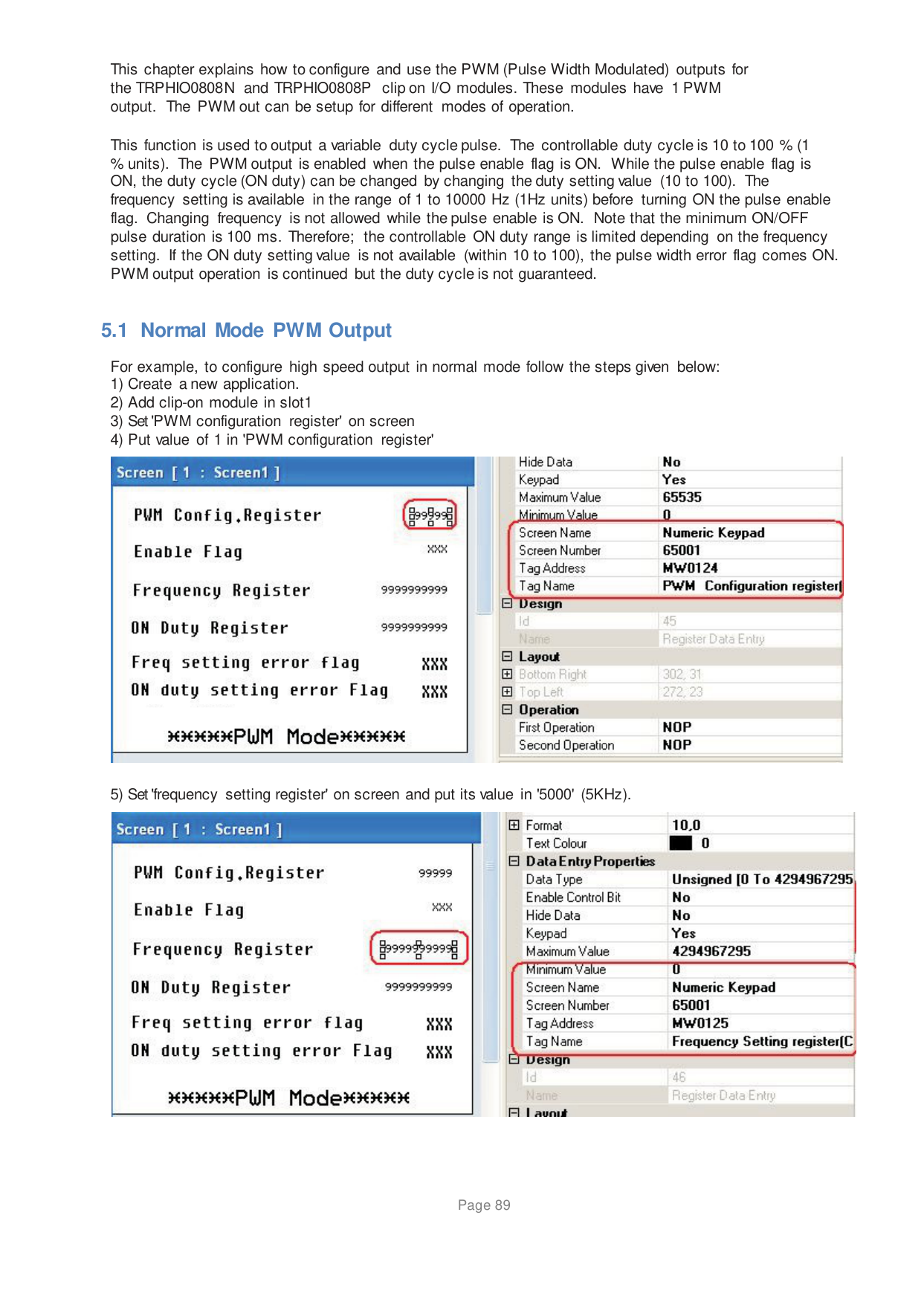
######### HIGH SPEED COUNTER INPUTS
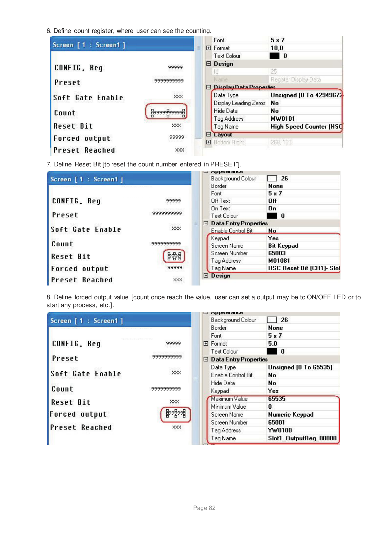
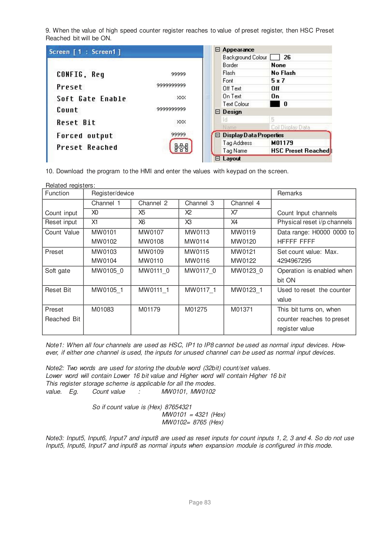
♦ High Speed Counter Setup
♦ Single Phase Counter
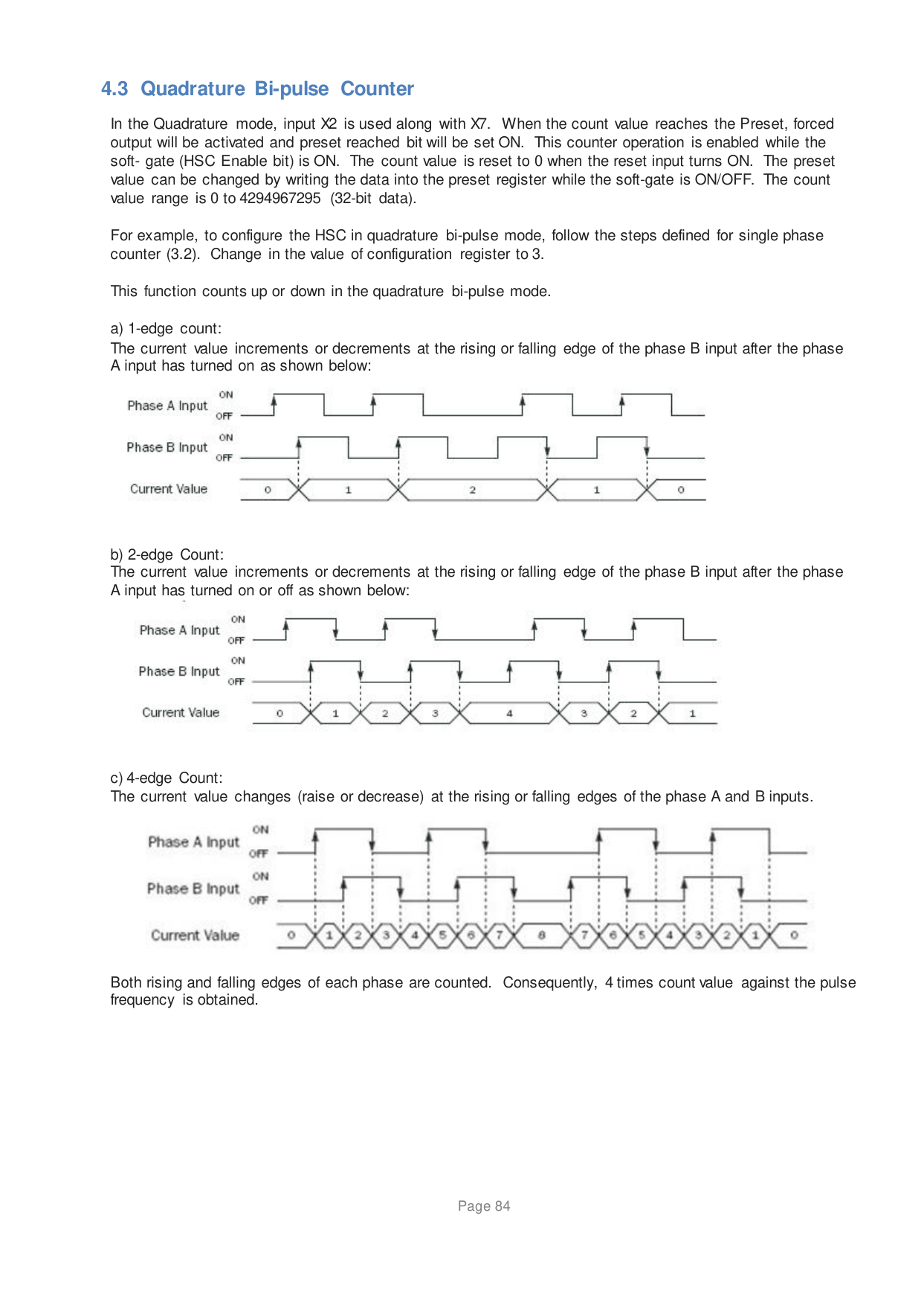
♦ Quadrature Bi-Pulse Counter
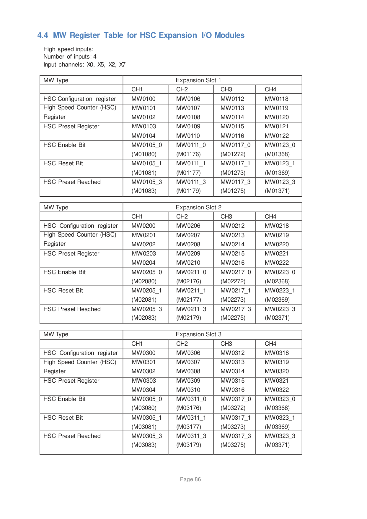
♦ MW Register Table for High Speed Counter Modules
############# 4.1 High Counter Setup
This chapter explains how to configure and use the HSC (High Speed Counter) inputs for the TRPHIO0808N and TRPHIO0808P clip on I/O modules. These modules have 4 HSC inputs. To configure the HSC inputs, follow the steps given below:

TRPHIO0808N


TRPHIO0808N

In this docker window,

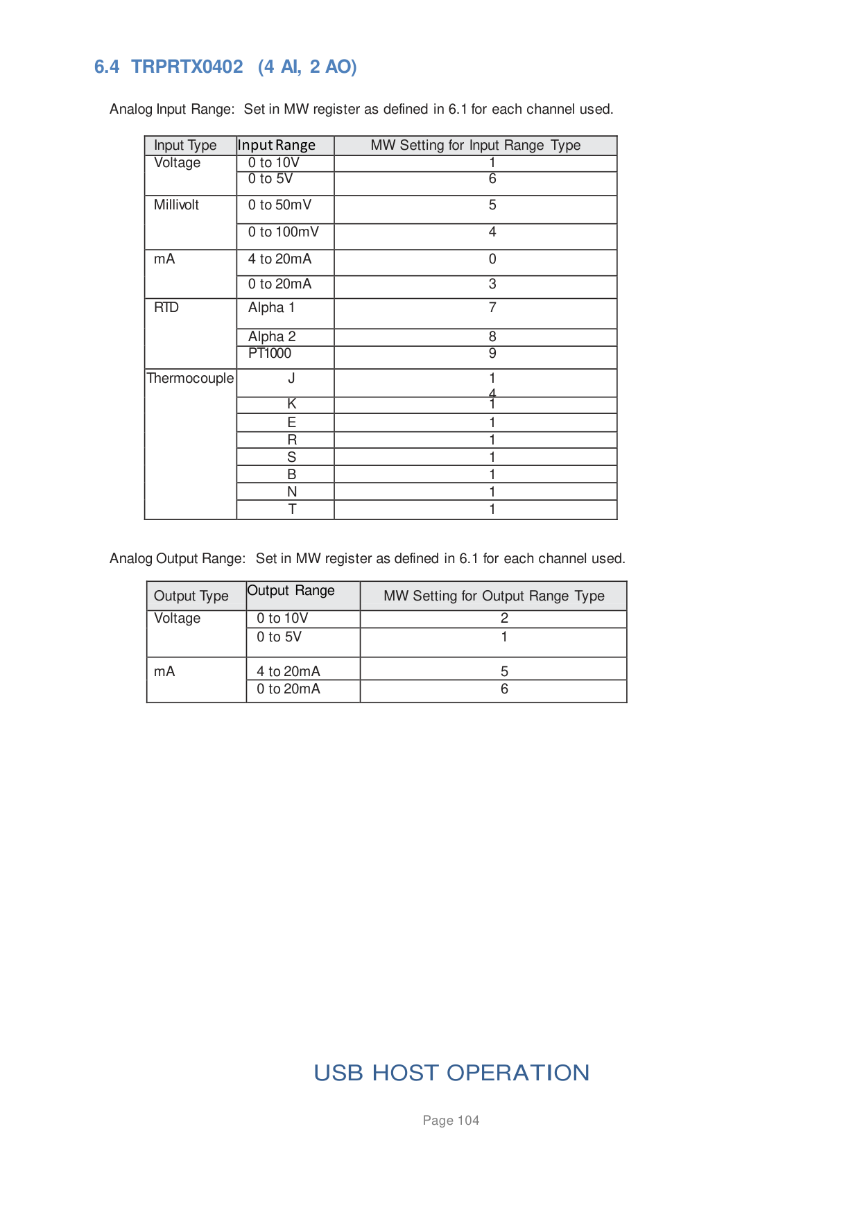
This option is “enabled”, by default. Once the user selects the HSC clip-on module, The default tags related to high speed counters will automatically be entered all as shown below:

Using this tag database, a user can setup different modes of the HSC.
############# 4.2 Single Phase Counter
[MWssrr Mode Select Bits = 010] When the count input is changed from OFF to ON, the count value is increased by 1. When the count value reaches the set value, the count value is reset to 0. This counter operation is enabled while the HSC enable bit is ON. The count value is reset to 0 when the Reset bit is changed from OFF to ON. The count value range is H0000 0000 to HFFFF FFFF (32-bit data).
For example, an application is given below:


The chart below shows the value for which HSC can RUN in different modes.

################## Normal Config HSC Condition Value in config register
################## r
Normal Input 0 HSC Single phase UP Counter Forced O/P ON preset reach 2
Forced O/P OFF preset reach, ON when enable
258

259
323
Quadrature 4X mode Forced O/P ON preset reach 131 Forced O/P OFF preset reach, ON when enable
387


| | |---|

| | |---|
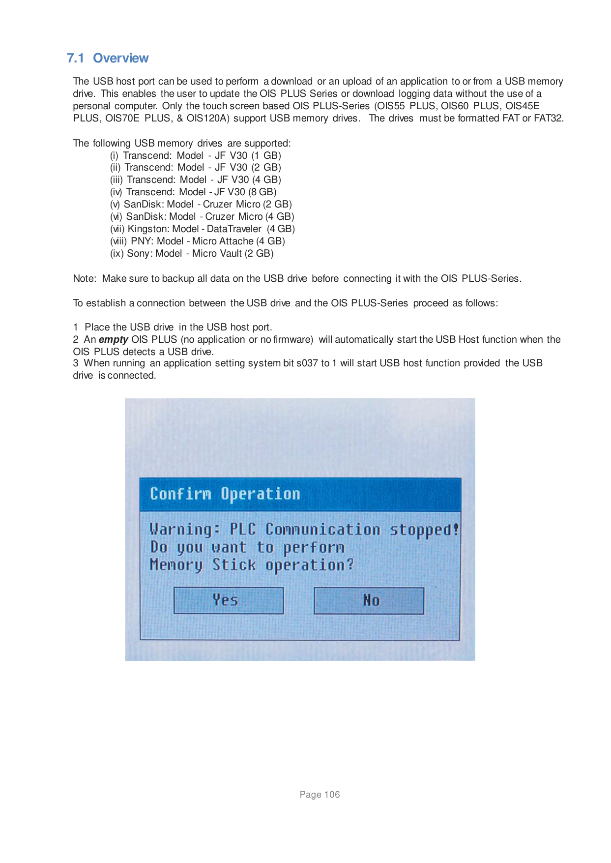

|Function|Register/device|Register/device|Register/device|Register/device|Remarks| |---|---|---|---|---|---| |Count input|Channel 1|Channel 2|Channel 3|Channel 4|Count Input channels| |Count input|X0|X5|X2|X7|Count Input channels| |Reset input|X1|X6|X3|X4|Physical reset i/p channels| |Count Value|MW0101
MW0102
|MW0107
MW0108
|MW0113
MW0114
|MW0119
MW0120
|Data range: H0000 0000 to HFFFF FFFF| |Preset|MW0103
MW0104
|MW0109
MW0110
|MW0115
MW0116
|MW0121
MW0122
|Set count value: Max. 4294967295| |Soft gate|MW0105_0|MW0111_0|MW0117_0|MW0123_0|Operation is enabled when bit ON| |Reset Bit|MW0105_1|MW0111_1|MW0117_1|MW0123_1|Used to reset the counter value| |Preset Reached Bit|M01083|M01179|M01275|M01371|This bit turns on, when counter reaches to preset register value|
So if count value is (Hex) 87654321
############# 4.3 Quadrature Bi-pulse Counter
In the Quadrature mode, input X2 is used along with X7. When the count value reaches the Preset, forced output will be activated and preset reached bit will be set ON. This counter operation is enabled while the soft- gate (HSC Enable bit) is ON. The count value is reset to 0 when the reset input turns ON. The preset value can be changed by writing the data into the preset register while the soft-gate is ON/OFF. The count value range is 0 to 4294967295 (32-bit data).
For example, to configure the HSC in quadrature bi-pulse mode, follow the steps defined for single phase counter (3.2). Change in the value of configuration register to 3.
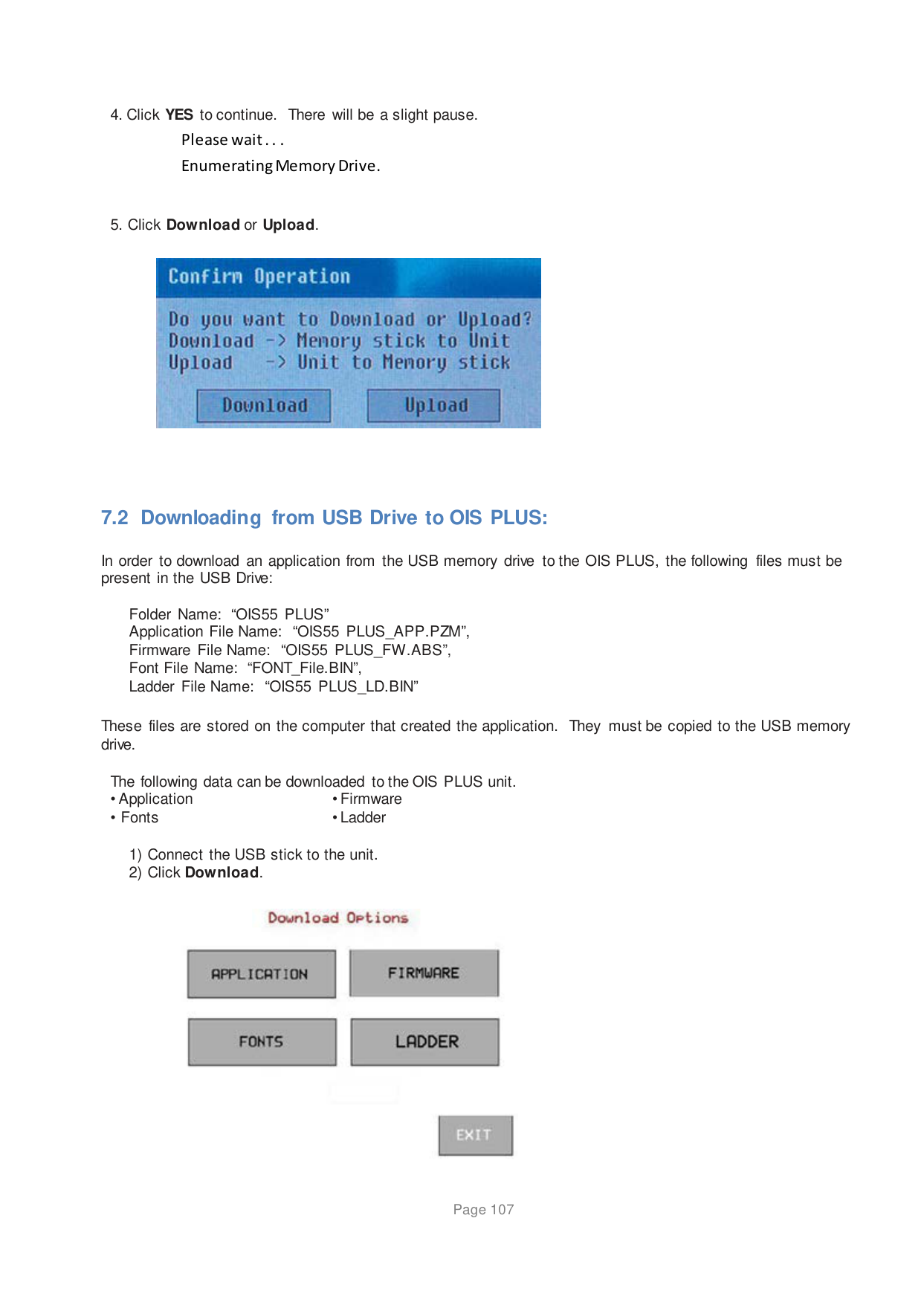
This function counts up or down in the quadrature bi-pulse mode.


Both rising and falling edges of each phase are counted. Consequently, 4 times count value against the pulse frequency is obtained.
Related registers: Function Device/Register Remarks
Preset MW0108 MW0109
Set Count Value: Max = 4294967295
Soft Gate M01076 Operation Enabled when Bit is ON Reset Bit M01273 Resets the Counter Value Preset Reached M01275 Turns on when Counter reaches Preset
Value
############# 4.4 MW Register Table for HSC Expansion I/O Modules
High speed inputs: Number of inputs: 4 Input channels: X0, X5, X2, X7
|MW Type|Expansion Slot 1|Expansion Slot 1|Expansion Slot 1|Expansion Slot 1|
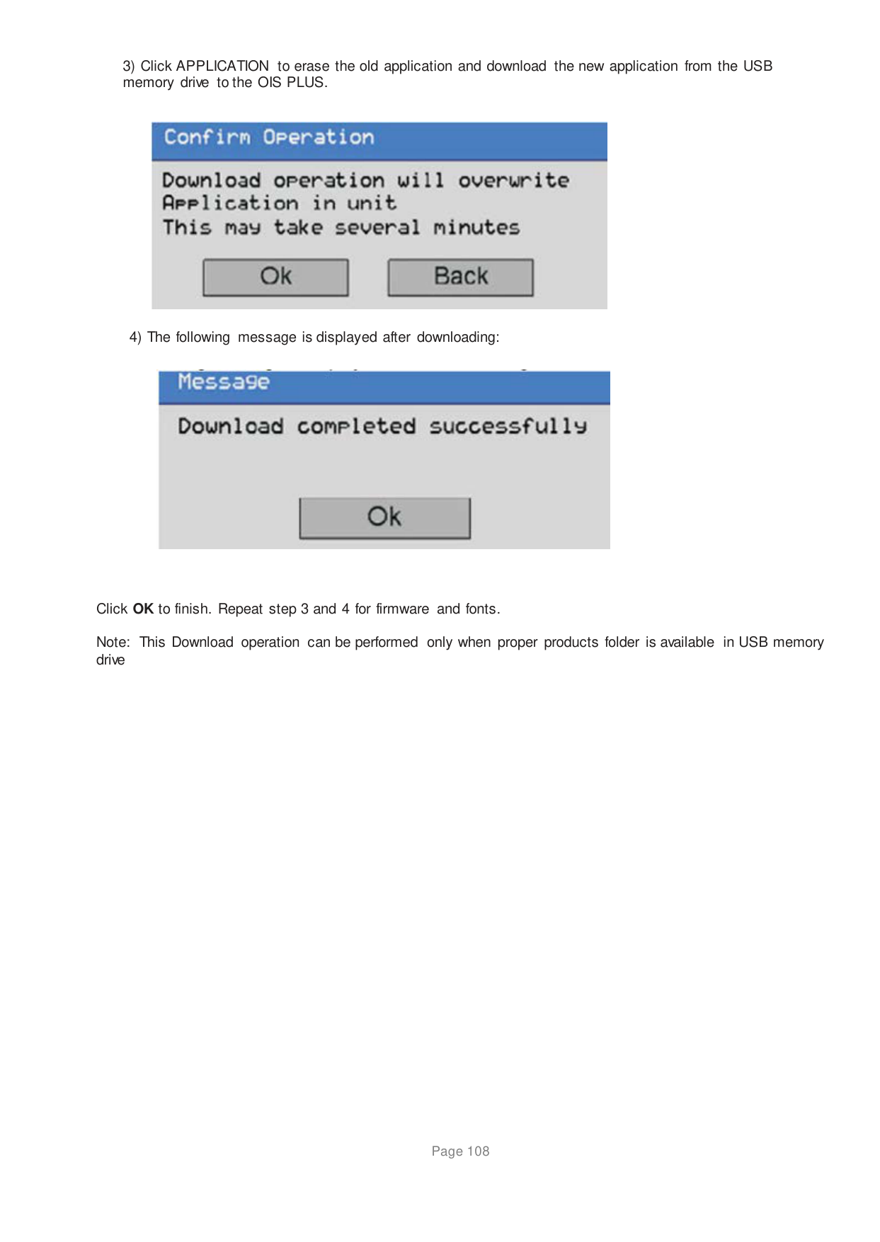
|---|---|---|---|---| | |CH1|CH2|CH3|CH4| |HSC Configuration register|MW0100|MW0106|MW0112|MW0118| |High Speed Counter (HSC) Register|MW0101
MW0102
|MW0107
MW0108
|MW0113
MW0114
|MW0119
MW0120
| |HSC Preset Register|MW0103
MW0104
|MW0109
MW0110
|MW0115
MW0116
|MW0121
MW0122
| |HSC Enable Bit|MW0105_0 (M01080)|MW0111_0 (M01176)|MW0117_0 (M01272)|MW0123_0 (M01368)| |HSC Reset Bit|MW0105_1 (M01081)|MW0111_1 (M01177)|MW0117_1 (M01273)|MW0123_1 (M01369)| |HSC Preset Reached|MW0105_3 (M01083)|MW0111_3 (M01179)|MW0117_3 (M01275)|MW0123_3 (M01371)|
|MW Type|Expansion Slot 2|Expansion Slot 2|Expansion Slot 2|Expansion Slot 2| |---|---|---|---|---| | |CH1|CH2|CH3|CH4| |HSC Configuration register|MW0200|MW0206|MW0212|MW0218| |High Speed Counter (HSC) Register|MW0201
MW0202
|MW0207
MW0208
|MW0213
MW0214
|MW0219
MW0220
| |HSC Preset Register|MW0203
MW0204
|MW0209
MW0210
|MW0215
MW0216
|MW0221
MW0222
| |HSC Enable Bit|MW0205_0 (M02080)|MW0211_0 (M02176)|MW0217_0 (M02272)|MW0223_0 (M02368)| |HSC Reset Bit|MW0205_1 (M02081)|MW0211_1 (M02177)|MW0217_1 (M02273)|MW0223_1 (M02369)| |HSC Preset Reached|MW0205_3 (M02083)|MW0211_3 (M02179)|MW0217_3 (M02275)|MW0223_3 (M02371)|
|MW Type|Expansion Slot 3|Expansion Slot 3|Expansion Slot 3|Expansion Slot 3| |---|---|---|---|---| | |CH1|CH2|CH3|CH4| |HSC Configuration register|MW0300|MW0306|MW0312|MW0318| |High Speed Counter (HSC) Register|MW0301
MW0302
|MW0307
MW0308
|MW0313
MW0314
|MW0319
MW0320
| |HSC Preset Register|MW0303
MW0304
|MW0309
MW0310
|MW0315
MW0316
|MW0321
MW0322
| |HSC Enable Bit|MW0305_0 (M03080)|MW0311_0 (M03176)|MW0317_0 (M03272)|MW0323_0 (M03368)| |HSC Reset Bit|MW0305_1 (M03081)|MW0311_1 (M03177)|MW0317_1 (M03273)|MW0323_1 (M03369)| |HSC Preset Reached|MW0305_3 (M03083)|MW0311_3 (M03179)|MW0317_3 (M03275)|MW0323_3 (M03371)|
|MW Type|Expansion Slot 4|Expansion Slot 4|Expansion Slot 4|Expansion Slot 4| |---|---|---|---|---| | |CH1|CH2|CH3|CH4| |HSC Configuration register|MW0400|MW0406|MW0412|MW0418| |High Speed Counter (HSC) Register|MW0401
MW0402
|MW0407
MW0408
|MW0413
MW0414
|MW0419
MW0420
|
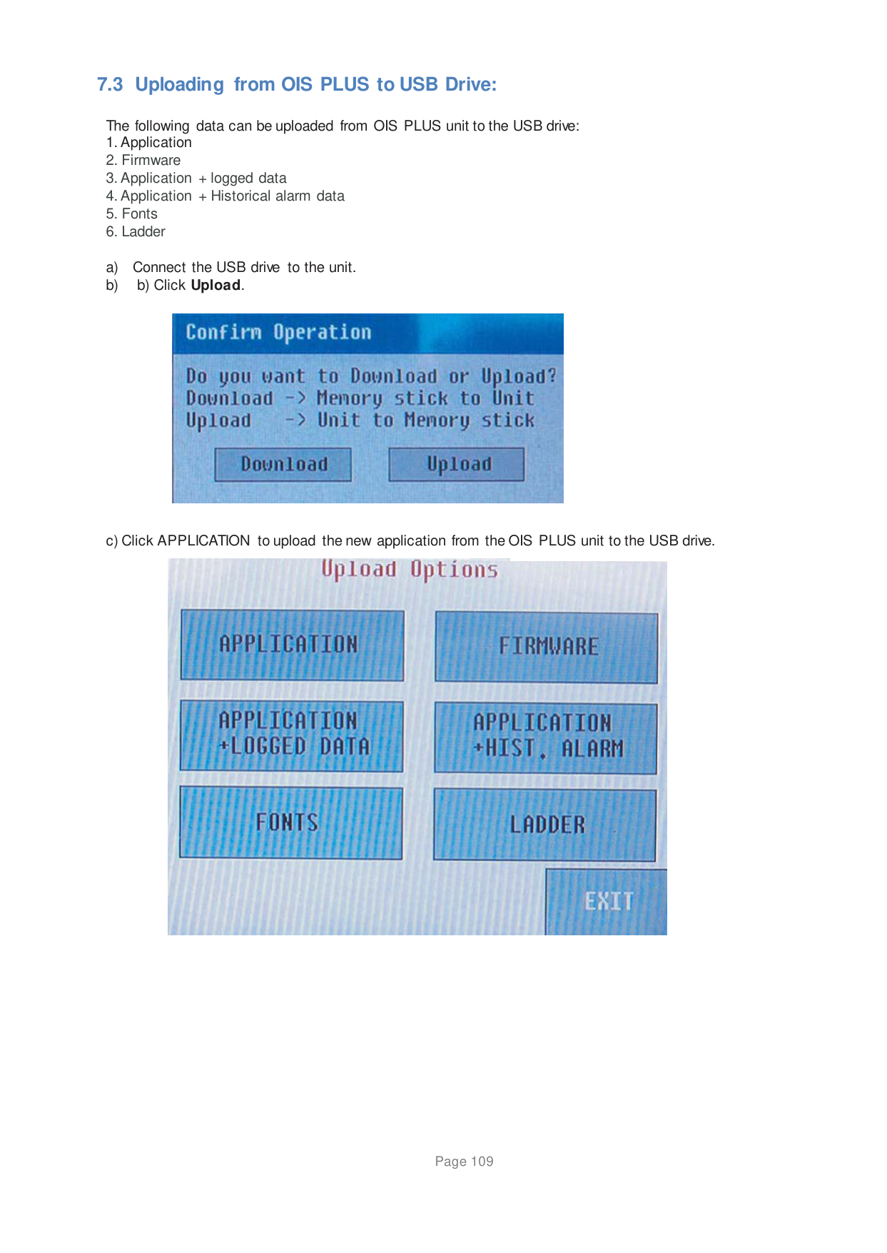
|HSC Preset Register|MW0403
MW0404
|MW0409
MW0410
|MW0415
MW0416
|MW0421
MW0422
| |HSC Enable Bit|MW0405_0 (M04080)|MW0411_0 (M04176)|MW0417_0 (M04272)|MW0423_0 (M04368)| |HSC Reset Bit|MW0405_1 (M04081)|MW0411_1 (M04177)|MW0417_1 (M04273)|MW0423_1 (M04369)| |HSC Preset Reached|MW0405_3 (M04083)|MW0411_3 (M04179)|MW0417_3 (M04275)|MW0423_3 (M04371)|
|MW Type|Expansion Slot 5|Expansion Slot 5|Expansion Slot 5|Expansion Slot 5| |---|---|---|---|---| | |CH1|CH2|CH3|CH4| |HSC Configuration register|MW0500|MW0506|MW0512|MW0518| |High Speed Counter (HSC) Register|MW0501
MW0502
|MW0507
MW0508
|MW0513
MW0514
|MW0519
MW0520
| |HSC Preset Register|MW0503
MW0504
|MW0509
MW0510
|MW0515
MW0516
|MW0521
MW0522
| |HSC Enable Bit|MW0505_0 (M05080)|MW0511_0 (M05176)|MW0517_0 (M05272)|M0W523_0 (M05368)| |HSC Reset Bit|MW0505_1 (M05081)|MW0511_1 (M05177)|MW0517_1 (M05273)|M0W523_1 (M05369)| |HSC Preset Reached|MW0505_3 (M05083)|MW0511_3 (M05179)|MW0517_3 (M05275)|MW0523_3 (M05371)|
################### Note: HSC Configuration register, High Speed Counter Register and HSC Preset register are retentive and will be retained at power down for all channels.
######### PULSE WIDTH MODULATED OUTPUTS
♦ Normal Mode PWM Output
♦ CW/CCW Mode PWM Output ♦ Pulse/DIR Mode PWM Output ♦ Fixed Pulse Mode PWM Output
############### ♦ MW Register Table for PWM I/O Modules
This chapter explains how to configure and use the PWM (Pulse Width Modulated) outputs for the TRPHIO0808N and TRPHIO0808P clip on I/O modules. These modules have 1 PWM output. The PWM out can be setup for different modes of operation.
This function is used to output a variable duty cycle pulse. The controllable duty cycle is 10 to 100 % (1 % units). The PWM output is enabled when the pulse enable flag is ON. While the pulse enable flag is ON, the duty cycle (ON duty) can be changed by changing the duty setting value (10 to 100). The frequency setting is available in the range of 1 to 10000 Hz (1Hz units) before turning ON the pulse enable flag. Changing frequency is not allowed while the pulse enable is ON. Note that the minimum ON/OFF pulse duration is 100 ms. Therefore; the controllable ON duty range is limited depending on the frequency setting. If the ON duty setting value is not available (within 10 to 100), the pulse width error flag comes ON. PWM output operation is continued but the duty cycle is not guaranteed.
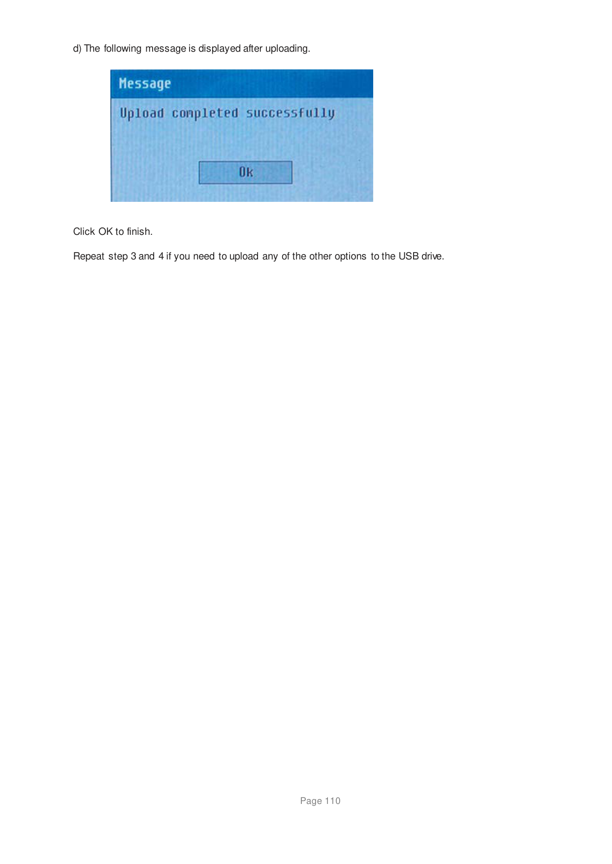


################### The function selection is done through configuration registers as follows:
|Function|Register / device Channel 1|Remarks| |---|---|---| |PWM pulse|Y2| | |Pulse enable flag|M136_0|Output is enabled when ON| |Frequency setting register|MW0125
MW0126
|Data range: 1 to 10000| |ON duty setting register|MW0127
MW0128
|Data range: 0 to 100| |Pulse width error flag|M129_1|ON at error (reset OFF automatically)| |ON duty setting error flag|M129_2|ON at error (reset OFF automatically)| |Frequency setting error flag|M129_3|ON at error (reset OFF automatically)|


This will RUN the operation in CW/CCW mode.
Note: The value of 'Frequency setting resister should be in between +/-1 to +/-10,000 If value of 'Frequency setting resister' is less than 1 or greater than 10,000 then, frequency setting error flag will be 'ON' otherwise it will be OFF.
When CW/CCW mode is selected and if frequency data range is positive, match output 6(MR6) will be selected so that pulses will be out on Y2 and if frequency data range is negative, match output 1(MR1) will be selected so that pulses will be out on Y4.
|Function|Register/device|Remarks| |---|---|---| |CW Pulse|Y2| | |CCW Pulse|Y4| | |Pulse enable flag|MW0136_0|Output is enabled when ON| |Frequency setting register|MW0125
MW0126
|Data range: -10000 to –1, 1 to 10000| |Frequency setting error flag|MW0129_3|ON at error (Reset OFF automatically)|


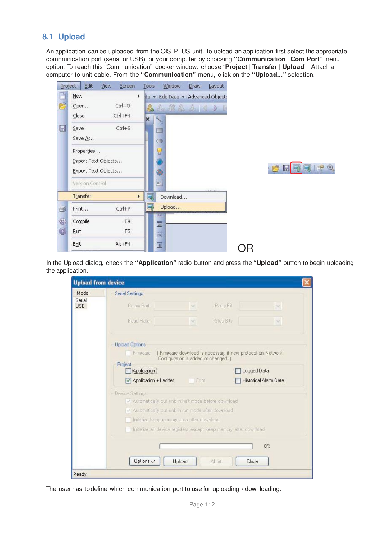

This will RUN the operation in Pulse/DIR
mode. Note: The value of 'Frequency setting resister should be in between +/-1 to +/-10,000. If value of 'Frequency setting resister' is less than 1 or greater than 10,000 then, frequency setting error flag will be 'ON' otherwise it will be OFF.
In PULSE/DIR mode the pulses will be out on Y2 i.e. Match output6 (MR6). If the frequency data range is negative then direction pin can be set to high through Match output 1(MR1).i.e. direction status can be out on Y4.
|Function|Register/device|Remarks| |---|---|---| |PLS|Y2| | |DIR|Y4| | |Pulse enable flag|MW0136_0|Output is enabled when ON| |Frequency setting register|MW0125
MW0126
|Data range: -10000 to –1, 1 to 10000| |Frequency setting error flag|MW0129_3|ON at error (Reset OFF automatically)|
################### Timing Diagram


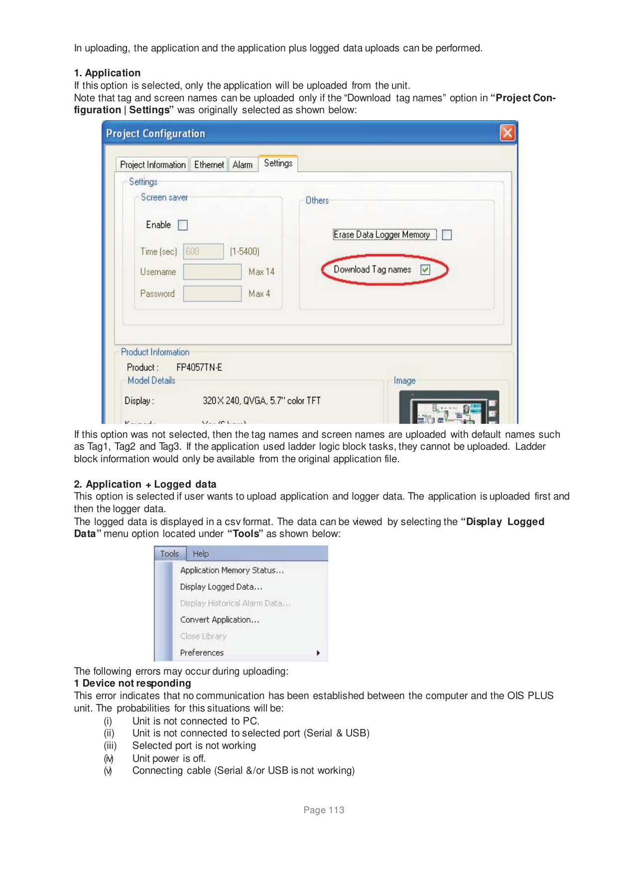

Note: Minimum frequency should be maximum 10,000.
In this mode, fixed number of pulses can be output on the Y2 of expansion of transistor outputs of the unit according to the specified parameter. The function selection is done using Configuration register MW0124 (for Slot 1).
When the corresponding control flag is off and the execution condition (trigger) is in the on state, a pulse is output from the specified output (Y2). The control code, minimum frequency, maximum frequency, acceleration time, deceleration time and total number of pulses are specified by a user program as shown in the following table. The frequency is switched by the acceleration/deceleration time specified for changing from the initial speed to the maximum speed. The acceleration and deceleration is normally done in 30 steps.


############# 5.5 MW Register Table for PMW I/O ModulesMW Register Table:
|Function|Register/device|Remarks| |---|---|---| |PWM pulse CH1|Y2|Expansion Y2| |Configuration Register|MW0124|Fixed pulse mode configuration register| |Pulse Out Enable|MW0136_0 (M01576)|Bit ‘0’ is used for enable High speed output.| |MIN Freq CH1|MW0125
MW0126
|Data range: 1 to 10000|
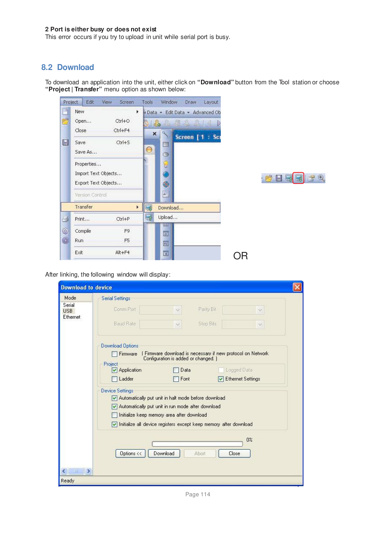
|MAXFreq CH1|MW0127
MW0128
|Data range: 1 to 10000| |Acceleration Time CH1|MW0137|0 to 32767 ( in mSec )| |Deceleration Time CH1|MW0139|0 to 32767 ( in mSec )| |Total Pulse CH1|MW0141
MW0142
|0 to + 2147483647| |Elapsed value CH1|MW0145
MW0146
|0 to + 2147483647 (Read / Write)| |Frequency Setting Error Flag CH1|MW0129_3 (M01467)|Turns ON at error (Bit ‘2’ of MW0129 register)| |Acceleration Time Setting error flag|MW0129_4 (M01468)|Turns ON at error| |Deceleration Time Setting error flag|MW0129_5 (M01469)|Turns ON at error| |No of Total Pulses Setting error flag|MW0129_6 (M01470)|Turns ON at error| |End of total pulses|MW0049_0 (M01784|Turns ON at the end of pulses.|
################### High speed outputs: Number of outputs: 1 Output channels: Y2, Y4
|MW Type
|Expansion Slot 1|Expansion Slot 2|Expansion Slot 3| |---|---|---|---| |MW Type
|CH1 (Y2)|CH1 (Y2)|CH1 (Y2)| |Configur ation.|MW0124|MW0224|MW0324| |Frequency|MW0125|MW0225|MW0325| |Setting register|MW0126|MW0226|MW0326| |ON duty setting register|MW0127
MW0128
|MW0227
MW0228
|MW0327
MW0328
| |Pulse Enable Flag|MW0136_0 (M01576)|MW0236_0 (M02576)|MW0336_0 (M03576)| |Pulse width error flag|MW0129_1 (M01465)|MW0229_1 (M02465)|MW0329_1 (M03465)| |ON duty setting error flag|MW0129_2 (M01466)|MW0229_2 (M02466)|MW0329_2 (M03466)| |Frequency setting error flag|MW0129_3 (M01467)|MW0229_3 (M02467)|MW0329_3 (M03467)| |Acceleration Time Setting error flag|MW0129_4 (M01468)|MW0229_4 (M02468)|MW0329_4 (M03468)| |Deceleration Time Setting error flag|MW0129_5 (M01469)|MW0229_5 (M02469)|MW0329_5 (M03469)| |No of Total Pulses Setting error flag|MW0129_6 (M01470)|MW0229_6 (M02470)|MW0329_6 (M03470)| |End of total pulses|MW0149_0 (M01784)|MW0249_0 (M02784)|MW0349_0 (M03784)|
|MW Type|Expansion Slot 4|Expansion Slot 5| |---|---|---| |MW Type|CH1 (Y2)|CH1 (Y2)| |Configure Register Frequency|MW0424; MW0425|MW0524; MW0525| |Setting register|MW0426|MW0526| |ON duty setting register|MW0427; MW0428|MW0527; MW0528|
|Pulse Enable Flag|MW0436_0 (M04576)|MW0536_0 (M05576)| |Pulse width error flag|MW0429_1 (M04465)|MW0529_1 (M05465)| |ON duty setting error flag|MW0429_2 (M04466)|MW0529_2 (M04466)| |Frequency setting error flag|MW0429_3 (M04467)|MW0529_3 (M04467)| |Acceleration Time Setting error flag|MW0429_4 (M04468)|MW0529_4 (M04468)| |Deceleration Time Setting error flag|MW0429_ 5|MW0529_5 (M04469)| |No of Total Pulses Setting error flag|MW0429_ 6|MW0529_6 (M04470)| |End of total pulses|MW0449_0 (M04784)|MW0549_0 (M05784)|
################### Configuration Register (Pulse/PWM Output): MWssrr


######### ANALOG MODULE SETUP
♦ Overview
♦ TRPAIO0400L (4 AI)
♦ TRPAIO0202L (2 AI, 2 AO)
♦ TRPRTX0402 (4 AI, 2 AO)
############# 6.1 Overview
OIS PLUS clip-on analog modules can accept a number of different types of inputs and produce different types of outputs. To determine which type of input and which type of output the module used, a profile for the modules must be setup in the MW registers. The group of MW registers assigned to the module is determined by the modules mounting position. The OIL-DS software is used to assigned values to the MW registers. The following table shows the relationship between the MW configuration registers, XW input registers, and the YW output registers.
|Register Description
|Register Description
|Expansion Slot|Expansion Slot|Expansion Slot|Expansion Slot|Expansion Slot| |---|---|---|---|---|---|---| |Register Description
|Register Description
|Slot1|Slot2|Slot3|Slot4|Slot5| |Input Registers
|Analog Input (CH0) Type- Slotxx|MW0100|MW0200|MW0300|MW0400|MW0500| |Input Registers
|Analog Input (CH1) Type- Slotxx|MW0101|MW0201|MW0301|MW0401|MW0501| |Input Registers
|Analog Input (CH2) Type- Slotxx|MW0102|MW0202|MW0302|MW0402|MW0502| |Input Registers
|Analog Input (CH3) Type- Slotxx|MW0103|MW0203|MW0303|MW0403|MW0503|
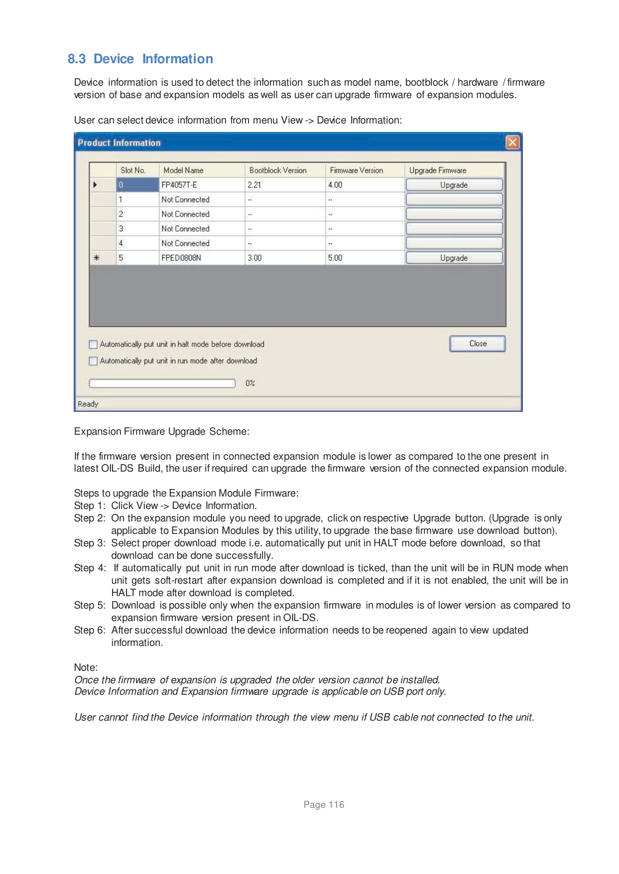
|Input Registers
|Input Register(CH0)Slotxx|XW0100
XW0101
|XW0200
XW0201
|XW0300
XW0301
|XW0400
XW0401
|XW0500
XW0501
| |Input Registers
|Input Register(CH1)Slotxx|XW0102
XW0103
|XW0202
XW0203
|XW0302
XW0303
|XW0402
XW0403
|XW0502
XW0503
| |Input Registers
|Input Register(CH2)Slotxx|XW0104
XW0105
|XW0204
XW0205
|XW0304
XW0305
|XW0404
XW0405
|XW0504
XW0505
| |Input Registers
|Input Register(CH3)Slotxx|XW0106
XW0107
|XW0206
XW0207
|XW0306
XW0307
|XW0406
XW0407
|XW0506
XW0507
| |Output Registers
|Analog Output (CH0) Type- Slotxx|MW0104|MW0204|MW0304|MW0404|MW0504| |Output Registers
|Analog Output (CH1) Type- Slotxx|MW0105|MW0205|MW0305|MW0405|MW0505| |Output Registers
|Output Register(CH0)Slotxx|YW0100|YW0200|YW0300|YW0400|YW0500| |Output Registers
|Output Register(CH1)Slotxx|YW0101|YW0201|YW0301|YW0401|YW0501|
All analog modules are configured as shown above depending on their slot number. Beyond the above each module must be setup individually.
Note: All settings are in decimal.
############# 6.2 TRPAIO0400L (4 AI)
Analog Input Range: Set in MW register as defined in 6.1 for each channel used.
|Sr. No|Input Range|MW Setting for Input Range Type| |---|---|---| |1|4 to 20mA|0| |2|0 to 10V|1| |3|-10 to 10V|2| |4|0 to 20mA|3|
Analog Output Range: None
############# 6.3 TRPAIO0202L (2 AI, 2 AO)
Analog Input Range: Set in MW register as defined in 6.1 for each channel used.
|Sr. No|Input Range|MW Setting for Input Range Type| |---|---|---| |1|4 to 20mA|0| |2|0 to 10V|1| |3|-10 to 10V|2|

|4|0 to 20mA|3|
Analog Output Range: Set in MW register as defined in 6.1 for each channel used.
|Sr. No|Output Range|MW Setting for Output Range Type| |---|---|---| |1|4 to 20mA|0| |2|0 to 10V|1| |3|0 to 20mA|3|
############# 6.4 TRPRTX0402 (4 AI, 2 AO)
Analog Input Range: Set in MW register as defined in 6.1 for each channel used.
|Input Type|Input Range|MW Setting for Input Range Type| |---|---|---| |Voltage|0 to 10V 0 to 5V|1 6| |Voltage| | | |Millivolt|0 to 50mV|5| |Millivolt|0 to 100mV|4| |mA|4 to 20mA|0| |mA|0 to 20mA|3| |RTD|Alpha 1|7| |RTD|Alpha 2|8| |RTD|PT1000|9| |Thermocouple
|J
K
|1 4 1| |Thermocouple
| | | |Thermocouple
|E|1| |Thermocouple
|R|1| |Thermocouple
|S|1| |Thermocouple
|B|1| |Thermocouple
|N|1| |Thermocouple
|T|1|
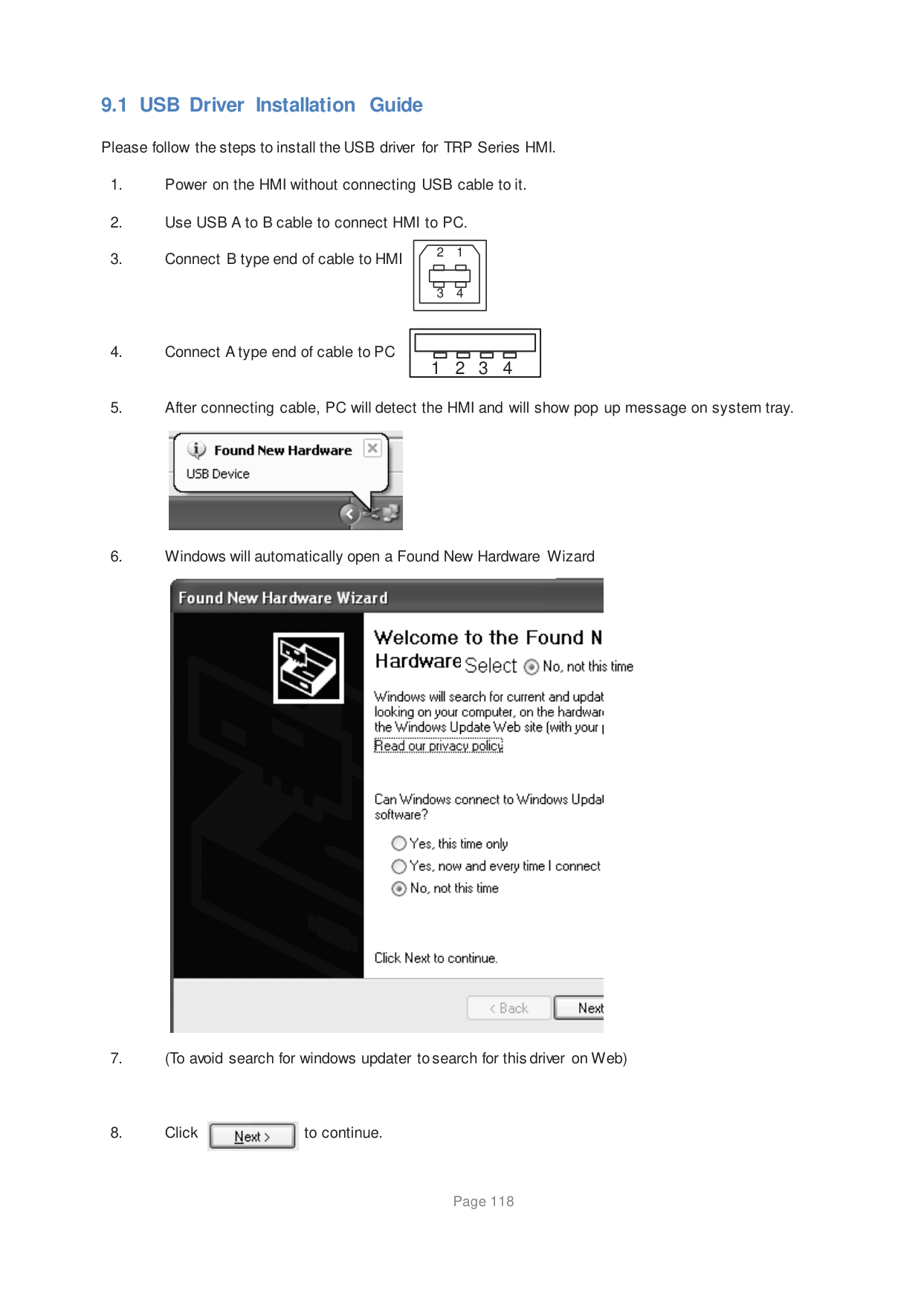
Analog Output Range: Set in MW register as defined in 6.1 for each channel used.
|Output Type|Output Range|MW Setting for Output Range Type| |---|---|---| |Voltage
|0 to 10V|2| |Voltage
|0 to 5V|1| |mA|4 to 20mA|5| |mA|0 to 20mA|6|
######### USB HOST OPERATION
♦ Downloading from USB Drive to OIS PLUS
♦ Uploading from OIS PLUS unit to USB Drive
############# 7.1 Overview
The USB host port can be used to perform a download or an upload of an application to or from a USB memory drive. This enables the user to update the OIS PLUS Series or download logging data without the use of a personal computer. Only the touch screen based OIS PLUS-Series (OIS55 PLUS, OIS60 PLUS, OIS45E PLUS, OIS70E PLUS, & OIS120A) support USB memory drives. The drives must be formatted FAT or FAT32.
The following USB memory drives are supported:
Note: Make sure to backup all data on the USB drive before connecting it with the OIS PLUS-Series.
To establish a connection between the USB drive and the OIS PLUS-Series proceed as follows:
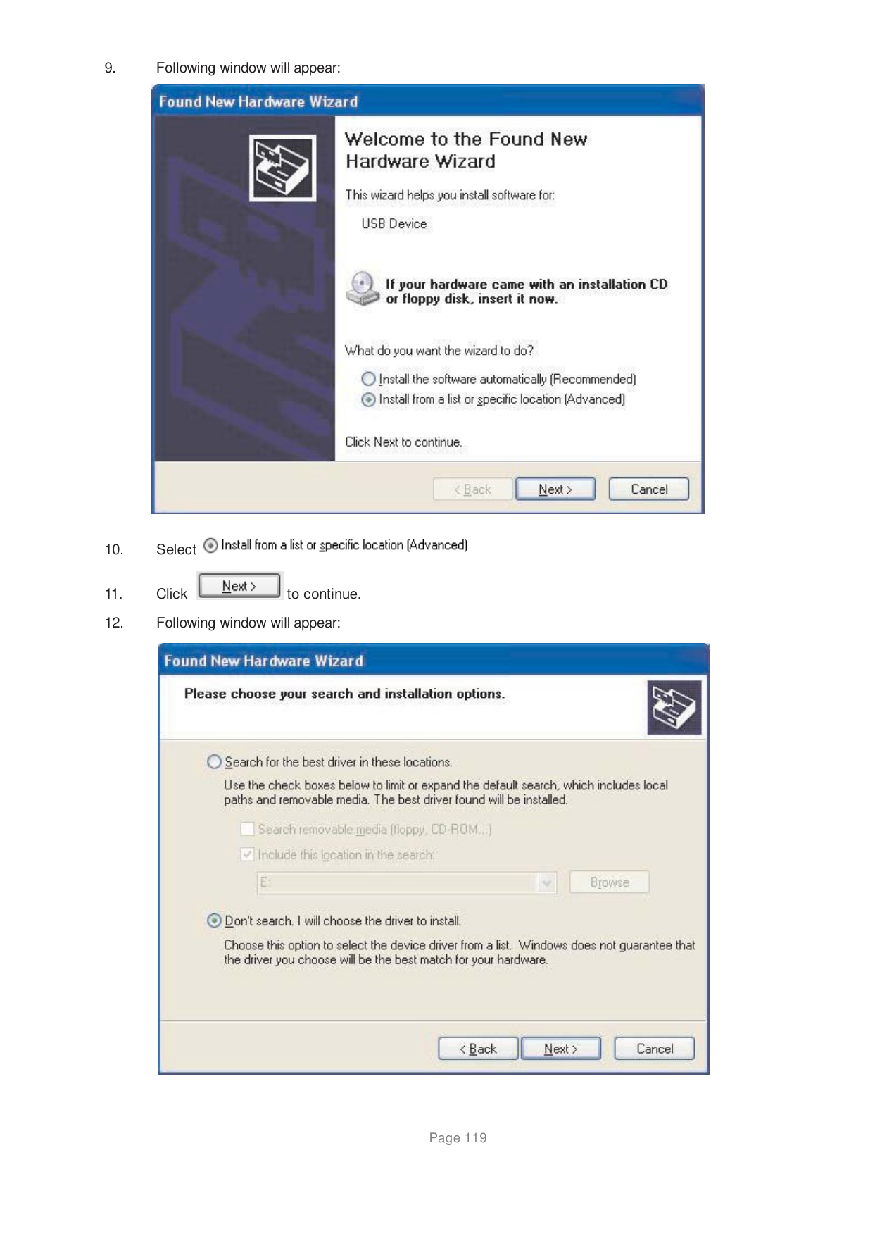


############# 7.2 Downloading from USB Drive to OIS PLUS:
In order to download an application from the USB memory drive to the OIS PLUS, the following files must be present in the USB Drive:
Folder Name: “OIS55 PLUS” Application File Name: “OIS55 PLUS_APP.PZM”, Firmware File Name: “OIS55 PLUS_FW.ABS”, Font File Name: “FONT_File.BIN”, Ladder File Name: “OIS55 PLUS_LD.BIN”
These files are stored on the computer that created the application. They must be copied to the USB memory drive.
The following data can be downloaded to the OIS PLUS unit.


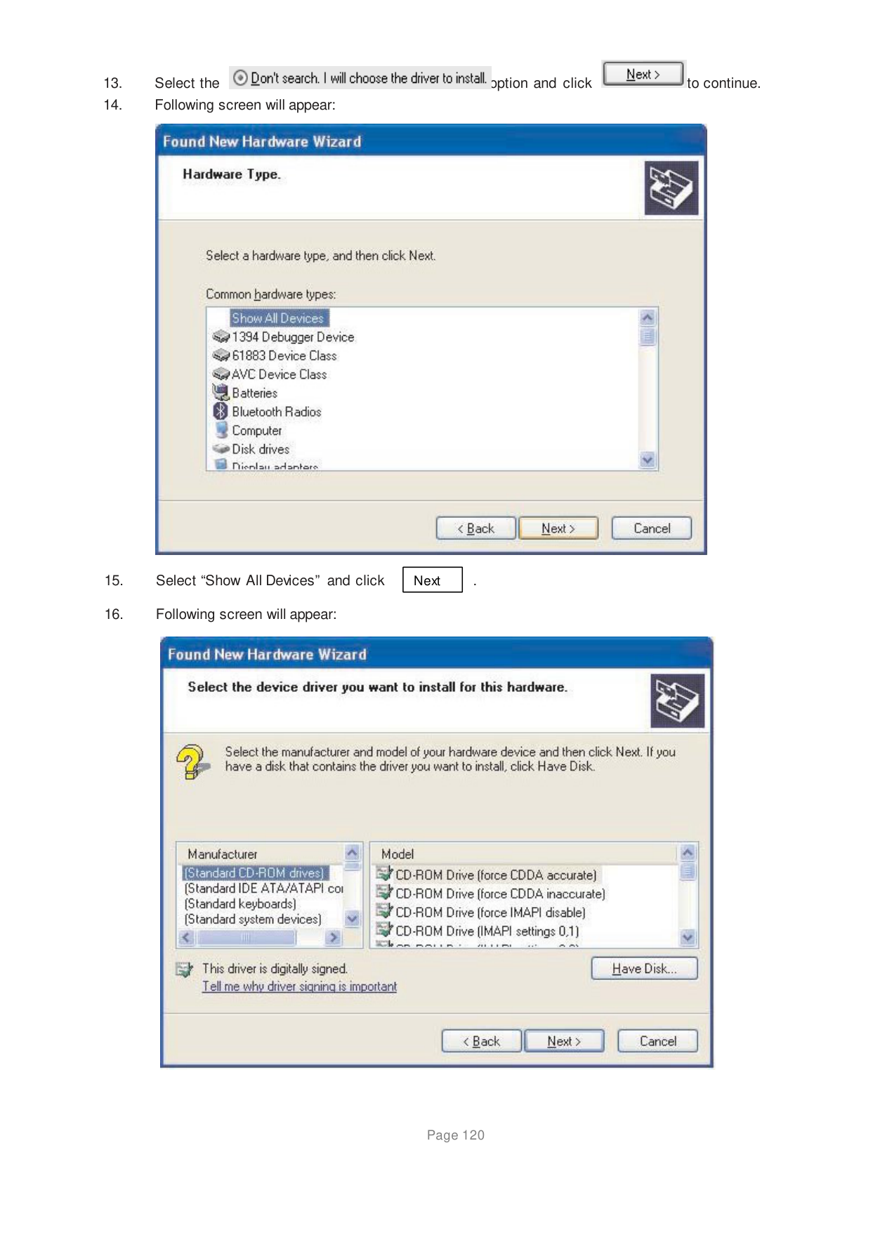


Click OK to finish. Repeat step 3 and 4 for firmware and fonts. Note: This Download operation can be performed only when proper products folder is available in USB memory drive
############# 7.3 Uploading from OIS PLUS to USB Drive:
The following data can be uploaded from OIS PLUS unit to the USB drive:


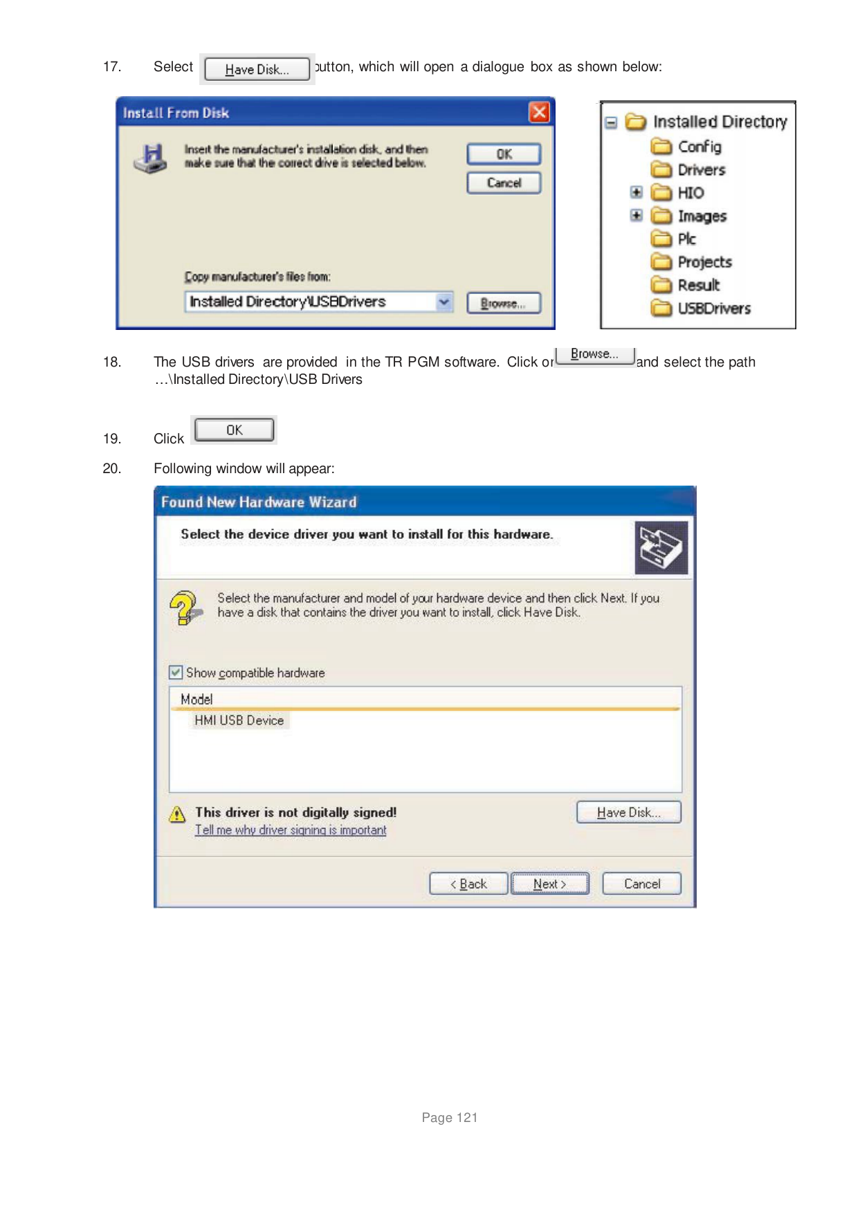


Click OK to finish.
Repeat step 3 and 4 if you need to upload any of the other options to the USB drive.
######### USB UPLOAD AND DOWNLOAD
♦ Upload an Application
♦ Download an Application
♦ Device Information
############# 8.1 Upload
An application can be uploaded from the OIS PLUS unit. To upload an application first select the appropriate communication port (serial or USB) for your computer by choosing “Communication | Com Port” menu option. To reach this “Communication” docker window; choose “Project | Transfer | Upload”. Attach a computer to unit cable. From the “Communication” menu, click on the “Upload...” selection.


####### OR
In the Upload dialog, check the “Application” radio button and press the “Upload” button to begin uploading the application.

The user has to define which communication port to use for uploading / downloading.
In uploading, the application and the application plus logged data uploads can be performed.
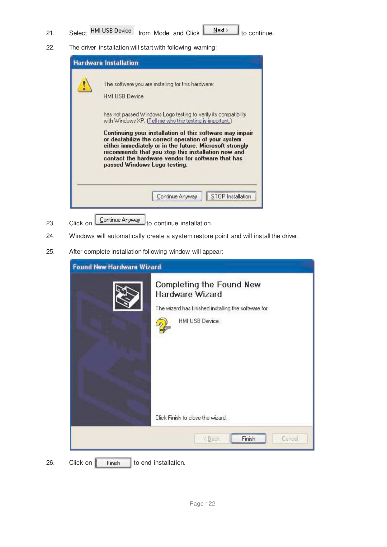
If this option was not selected, then the tag names and screen names are uploaded with default names such as Tag1, Tag2 and Tag3. If the application used ladder logic block tasks, they cannot be uploaded. Ladder block information would only be available from the original application file.


The following errors may occur during uploading:
############# 8.2 Download
To download an application into the unit, either click on “Download” button from the Tool station or choose “Project | Transfer” menu option as shown below:


######## OR
After linking, the following window will display:

Com Port – Used to select which communication port to use for downloading. By default Com1 is selected. Any changes are stored with the OIS PLUS program.
Download Options
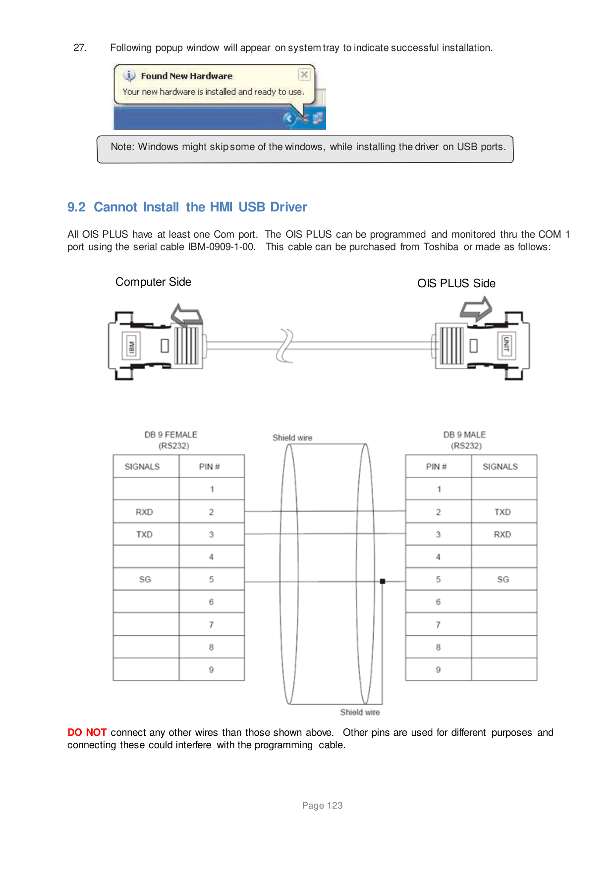
Note: At Power Cycle Only the User specified Keep memory Area is retained and other device Registers are initialized to Zero. Download options are applicable only at the time of Download of Program.
Download Button - Click this button to start the downloading.
Abort Button - Click on this button to stop the downloading.
The following errors may occur during Downloading:
############# 8.3 Device Information
Device information is used to detect the information such as model name, bootblock / hardware / firmware version of base and expansion models as well as user can upgrade firmware of expansion modules.
User can select device information from menu View -> Device Information:


Expansion Firmware Upgrade Scheme:
If the firmware version present in connected expansion module is lower as compared to the one present in latest OIL-DS Build, the user if required can upgrade the firmware version of the connected expansion module.
Steps to upgrade the Expansion Module Firmware:
Note: Once the firmware of expansion is upgraded the older version cannot be installed. Device Information and Expansion firmware upgrade is applicable on USB port only.
User cannot find the Device information through the view menu if USB cable not connected to the unit.
######### USB DRIVER INSTALLATION
############# 9.1 USB Driver Installation Guide
Please follow the steps to install the USB driver for TRP Series HMI.
|2 1
| | | | | | |---|---|---|---|---| | | | | | | | | | | | |
3 4
|

|---|
|| | |---|
1 2 3 4| |---|


Next


b


n


Note: Windows might skip some of the windows, while installing the driver on USB ports.
############# 9.2 Cannot Install the HMI USB Driver
All OIS PLUS have at least one Com port. The OIS PLUS can be programmed and monitored thru the COM 1 port using the serial cable IBM-0909-1-00. This cable can be purchased from Toshiba or made as follows:
Computer Side OIS PLUS Side


DO NOT connect any other wires than those shown above. Other pins are used for different purposes and connecting these could interfere with the programming cable.


############## TOSHIBA INDUSTRIAL PRODUCTS:


© 2011 Toshiba International Corporation Industrial Division • 13131 West Little York Road Houston, Texas 77041 USA • Tel +713-466-0277 US 1-800-231-1412 •